Products & Technologies
Products & Services
Contact
Back to Menu
Products & Services
Products & Technologies
Services
Resources
Contact
Posted
June 24, 2024

Stay updated on our content.
Power-Hungry AI Applications Demand More Energy-Efficient Computing

by Mukund Srinivasan
June 24, 2024
The computing industry’s relentless pursuit of more capable artificial intelligence is triggering the need for major inflections in logic and memory. While data center AI is expected to eclipse PCs and then smartphones as the number one driver of leading-edge foundry-logic and DRAM wafer starts, the growth of AI may be gated by the limits of the power grid – and push carbon neutrality goals years into the future – unless we dramatically improve the efficiency of chips and systems.
A recent report from Goldman Sachs projects that data center power consumption could grow dramatically in the coming years, producing a level of electricity demand not seen in a generation. While data center power demand has been relatively flat for many years, the study predicts that it could grow by 160 percent from 2023 to 2030, ultimately accounting for up to four percent of global power demand while more than doubling carbon dioxide emissions compared to 2022. This surge in demand threatens to undo our collective efforts to build a more sustainable electronics industry.
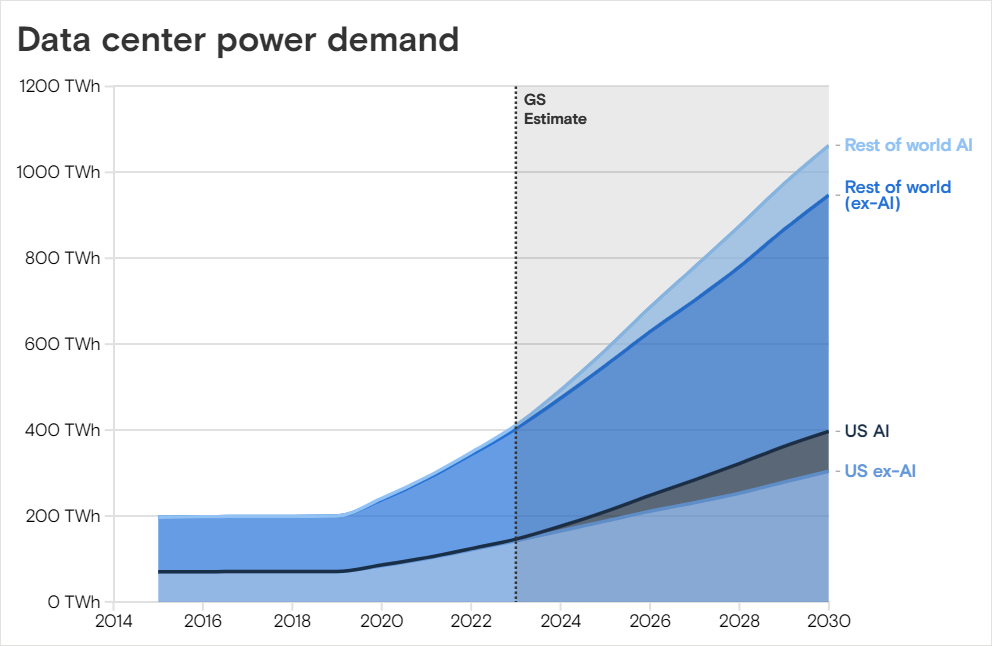
Global Data Center Electricity Consumption. Source: Masanet et al. (2020), Cisco, IEA, Goldman Sachs Global Investment Research
As noted in a recent IEEE Spectrum article co-authored by TSMC chairman Dr. Mark Liu and chief scientist Dr. H.-S. Philip Wong, the rise of AI is driven in large part by advances in semiconductor technologies. Over the past 15 years, our industry has delivered innovations that increased energy-efficient performance about threefold every two years. To understand how we can maintain this historic trend to support the sustainable growth of AI, let’s take a brief look at how the industry has tackled the performance-per-watt challenge.
A Brief History of Chip Scaling
Decades ago, two-dimensional shrinking with Dennard scaling produced simultaneous improvements in power, performance and area-cost. The approach worked using conventional materials such as silicon, silicon oxide, nitride and aluminum – until roughly the 90nm technology node.
Over time, Dennard scaling continued to deliver performance and area-cost savings, but power scaling came to a halt. Interconnect performance hit a bottleneck, and the era of materials-enabled devices was born. To overcome resistive-capacitive delay, for example, the industry replaced aluminum wires with copper and introduced “low-k” dielectrics as insulating materials between the wires. After 20 more years, manufacturers drove another materials inflection with the adoption of more exotic materials such as cobalt and novel processes including selective barriers and capping layers to enable continued scaling of copper interconnects.
Transistor performance became the next bottleneck due to channel mobility and gate leakage, which heralded the use of epitaxially grown materials that employ strain engineering to achieve higher carrier mobility and new high-k dielectrics and metals for the transistor gate to reduce leakage. This next wave of materials solutions aided the transition from planar to 3D FinFET transistors, while new selective removal steps, new material treatment steps and new ALD metal gate stack materials were used to improve performance and power.
More recently, innovations in materials engineering are enabling scaling into the “angstrom era,” where critical dimensions are truly approaching the level of individual atoms and molecules. Here, materials behave entirely differently as a result of the increased surface-volume ratio, quantum effects, enhanced reactivity and structural changes – requiring more care and attention through vacuum clustering and precision engineering of materials and surfaces. As we enter this new era, precision engineering of materials and surfaces is enabling the next generation of transistor and interconnect innovations, with chipmakers transitioning to new Gate-All-Around (GAA) transistor architectures and Backside Power Delivery (BPD) wiring schemes.
Advanced packaging is another scaling solution that requires new materials and system integration to bring different chips closer together – such as logic and DRAM – for higher bandwidth, lower latency and better energy efficiency.
Continued Innovation for More Energy-Efficient Computing
As the performance demands of AI systems continue to increase, the semiconductor equipment industry has a critical role to play in enabling chipmakers to continue scaling with improvements in power as well as performance.
On July 9 at our SEMICON West Technology Breakfast event, Applied Materials will demonstrate how the semiconductor manufacturing ecosystem can enable better AI through materials engineering. First, Mark Fuselier, SVP of technology and product engineering at AMD, will share his company's AI computing technology vision for a world that demands continuous improvements in performance-per-watt. Then, Applied's experts will discuss our advanced materials engineering roadmap and how it can help make future logic and memory chips for AI chips even faster and more power efficient.
Together with our customers, we are working on breakthrough chip and system solutions for the computing industry – enabling more energy-efficient AI.
Mukund Srinivasan
Group Vice President and General Manager - Etch Business Unit and Integrated Module Solutions Group

Dr. Mukund Srinivasan is the Group Vice President and General Manager for the Etch Business Unit and Integrated Module Solutions Group. Prior to joining Applied in 2013, Dr. Srinivasan spent 16 years at Lam Research in different positions, including General Manager for the Clean Product Group and leadership positions in Etch. He holds a Ph.D. in mechanical engineering from the University of California, Berkeley.
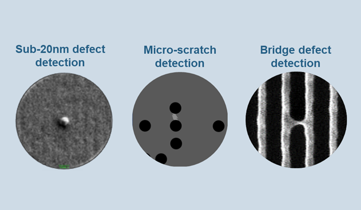
Advanced Logic and Memory Need New Tools for Optical Wafer Inspection
The journey from R&D to high-volume manufacturing is a race, and whoever crosses the finish line first wins competitive advantage in terms of revenue, market share and profitability. Advanced chips are built up one layer at a time, and each of the billions of individual features must be perfectly patterned and aligned to create working transistors and interconnects with the best performance and power characteristics.
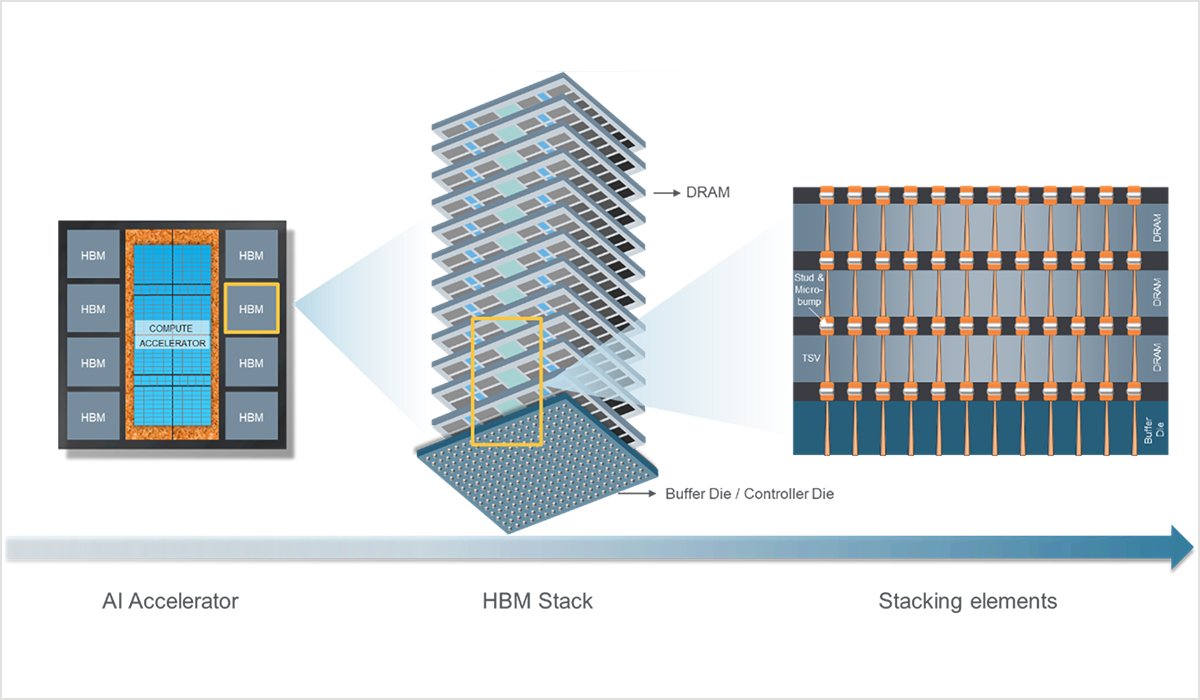
HBM: Materials Innovation Propels High-Bandwidth Memory Into the AI Era
Nvidia’s CEO Jensen Huang famously referred to the launch of OpenAI’s ChatGPT as an “iPhone moment” for artificial intelligence, describing it as “one of the greatest things that has ever been done for computing.”
Building on an Unmatched Foundation of CVD Innovation
Applied Materials recently celebrated the shipment of our 10,000th CVD system. For more than 30 years, Applied has introduced a steady stream of product and material innovations that have transformed the CVD semiconductor equipment market. With our latest CVD product innovation, the Producer® XP Pioneer® CVD patterning film, we are positioned to enable the next generation of inflections in both memory and logic.