Products & Technologies

Products & Services
Company
Contact
Back to Menu
Products & Services
Products & Technologies
Services
Resources
Company
Contact
Posted
February 23, 2018

Stay updated on our content.
Patterning Challenges and Opportunities at SPIE Advanced Lithography Symposium
Feb 23, 2018
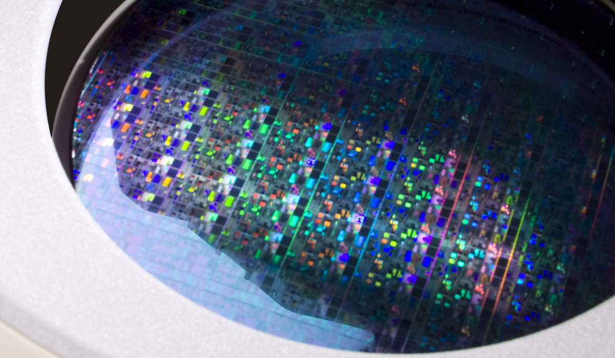
Technologists from across the semiconductor industry will gather in San Jose, Calif. next week for the 2018 SPIE Advanced Lithography symposium to discuss the latest advancements in lithography, metrology, patterning technologies and materials.
Applied Materials is presenting several papers focused on solving the industry’s toughest challenges in device scaling, including edge placement error (EPE) — the misalignment of critical features on one layer with features on other layers — mask and wafer defects, line edge roughness and critical dimension variations to help improve device performance and yield.
We look forward to sharing our findings and hope to see you at the conference!
ADVANCES IN PATTERNING MATERIALS AND PROCESSES CONFERENCE
Session 11, Sunday, Feb. 25, 3:40 to 5:00 PM
“DSA process characterization using BSE metrology,” CEA-LETI, Applied Materials. Direct Self Assembly (DSA) patterning offers a cost-effective manufacturing method to support pattern shrinks for advanced technology nodes. However, DSA pattern fidelity issues caused by dislocations can impact pattern fidelity after etch. In this paper, we highlight the usage of back scattered electron (BSE) metrology as an innovative approach to characterize the DSA process.
METROLOGY, INSPECTION, PROCESS CONTROL FOR MICROLITHOGRAPHY CONFERENCE
Session PS1 Tuesday, Feb. 26, 5:30 to 7:30 PM
“EUV lithography qualification: comparison of alternative wafer inspection methodologies and sensitivities,” Applied Materials. Defect inspection sensitivity on EUV absorber defects programmed on a test mask with design rules down to 16nmHP was studied using a defect review scanning electron microscope (DRSEM). Defect detection sensitivity was compared between DUV mask inspection and optical wafer inspection with a goal of detecting 10% critical dimension (CD) variation defects.
Session 8, Wednesday, Feb. 28, 8:00 to 10:00 AM
“Line roughness holistic metrology sensitivity study supported by EUV mask designed with induced roughness,” Applied Materials. Characterization of pattern roughness is crucial for yield and device performance. While CDSEM has been the main work horse for roughness measurements, this in-line metrology reference is limited in its ability to evaluate roughness measurement sensitivity. This paper reports on a novel approach to evaluate sensitivity and explore methods of signal enhancements on printed pattern wafers at different process steps.
Session PS2, Wednesday, Feb. 28, 5:30 to 7:30 PM
“Automated mask and wafers defects classification using a novel method for generalized CD variation measurements,” Applied Materials. Mask defects dispositioning has become a challenging and time-consuming task. While CD variation measurement is still the method of choice for determining the future impact of a mask defect on the wafer, the complexity of OPCs combined with high variability in pattern shapes pose a challenge for any automated CD variation measurement method. In this study, a novel approach for measurement generalization is presented.
Session 13, Thursday, Mar. 1, 11:10 to 11:30 AM
“Minimizing EUV edge placement error by fast high-resolution SEM,” IMEC, Applied Materials. Minimizing EPE challenges in SEM technology in three dimensions: resolution, throughput and applications. This paper shows how using a SEM platform addresses these challenges in a case using EUV. EUV lithography poses EPE challenges related to a different stochastic behavior relative to ArFi lithography. Massive sampling made possible by the SEM platform was used to characterize the unique random nature of EUV lithography in addition to other EPE contributors.
Tags: SPIE, lithography, Patterning, metrology, e-beam
Applied Materials Blog
Corporate Communications
The Applied Materials Blog team publishes blog posts of general interest to our readers.

Adding Sustainability to the Definition of Fab Performance
To enable a more sustainable semiconductor industry, new fabs must be designed to maximize output while reducing energy consumption and emissions. In this blog post, I examine Applied Materials’ efforts to drive fab sustainability through the process equipment we develop for chipmakers. It all starts with an evolution in the mindset of how these systems are designed.

Innovations in eBeam Metrology Enable a New Playbook for Patterning Control
The patterning challenges of today’s most advanced logic and memory chips can be solved with a new playbook that takes the industry from optical target-based approximation to actual, on-device measurements; limited statistical sampling to massive, across-wafer sampling; and single-layer patterning control to integrative multi-layer control. Applied’s new PROVision® 3E system is designed to enable this new playbook.

Breakthrough in Metrology Needed for Patterning Advanced Logic and Memory Chips
As the semiconductor industry increasingly moves from simple 2D chip designs to complex 3D designs based on multipatterning and EUV, patterning control has reached an inflection point. The optical overlay tools and techniques the semiconductor industry traditionally used to reduce errors are simply not precise enough for today’s leading-edge logic and memory chips.