Products & Technologies
Products & Services
Contact
Products & Services
Products & Technologies
Services
Resources
Contact
Posted
October 22, 2021

Stay updated on our content.
Now is the Time for Flat Optics

by Dante Zakhidov, Paul Gallagher, David Sell, Ph.D., Robert Visser, Ph.D.
Oct 22, 2021
Applied Materials’ recent Open Innovation Workshop on Flat Optics convened leading academic and industry experts to answer two main questions: 1) what are the applications of metasurfaces that differentiate them from traditional optics and 2) how close is the technology to commercial maturity? In this blog, we’ll highlight key learnings from the workshop and explain why Applied is excited about the future of flat optics. But first, a quick primer.
What are Flat Optics?
Traditional optics are based on the refraction and reflection of light in optical elements whose dimensions are significantly larger than the wavelengths of light they manipulate. The distinguishing feature of flat optics is the use of arrays of nanoscale elements that are now smaller than the wavelength of light they control (see Figure 1). In aggregate, these elements can bend and manipulate light to mimic the functionalities of traditional optics, but importantly, can also give rise to completely new capabilities.
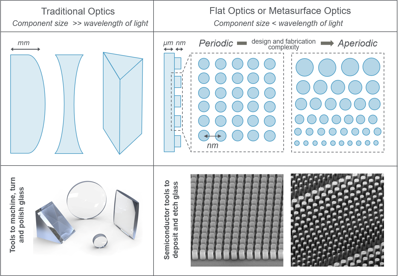
Figure 1: The distinguishing feature between traditional and flat optics is the component size relative to the wavelength of light.
“Flat optics is an area that is really rich with opportunities. It’s a very different way of guiding light and making light do tricks and things that we never imagined because they aren’t possible with bulk optics,” says Professor Stephen Forrest.
What are the Applications?
Flat optics research started with a focus on replacing and miniaturizing the functionality of bulk optics, but that’s just the tip of the iceberg. As research continued, new possibilities emerged beyond miniaturizing bulky glass lenses, including polarization imaging, biosensing, beam steering for automotive, and extended depth-of-focus lenses in flat cameras.
In terms of replacing traditional lenses, Professor Federico Capasso discussed at the workshop how we can use clever design of multilayered metasurfaces to enable lensing of multiple discrete wavelengths, such as in an RGB lens. Professor Jonathan Fan showed how it’s possible to set geometric boundary constraints within machine learning algorithms to design fabrication-feasible metasurfaces. Beyond basic lensing, flat optics will enable us to image frequency and amplitude as well as polarization, angular momentum and phase of light in new classes of small form-factor cameras.
Describing applications beyond imaging, Professor Arka Majumdar explained how flat optics can help with acceleration of machine learning as a hardware-based edge-detection layer. Other presented examples include, Professor Andrea Alu asserting how metasurfaces can shape the wavefront of light for augmented reality applications; Professor Andrei Faraon illustrating designed metaoptics as keys in security applications; and Professor Jennifer Dionne describing metasurfaces as a platform technology for highly sensitive and inexpensive sensors for a variety of biomarkers.
All the applications listed above were done using passive components; however, one of the most exciting aspects of flat optics is its compatibility with active materials. Professor Harry Atwater and Professor Mark Brongersma showed how active control of the metasurface materials could enable components for LIDAR, LiFi, holographic displays, additive manufacturing and new scientific instrumentation.
Is Flat Optics Reaching Commercial Viability?
Applied Materials, through the Office of the CTO and funding from Applied Ventures, is using its expertise in materials, high-throughput equipment design and process control at the nanoscale to help drive flat optics technology into a variety of volume markets.
“Applied can play at many levels but I think what they really bring that very, very few companies can in the world today is the ability to develop processes that control materials at the nanoscale,” says Professor Forrest.
With different materials challenges in flat optics compared to conventional silicon, from using glass substrates to different processing sequences and lithographic requirements, it’s important to be able to build suitable processes together with designs.
The unique properties of metasurface-based optics are generating increasing interest from both new companies and large corporations, providing evidence of flat optics’ potential across the commercialization value chain. Invited startups to the workshop showcased several compelling applications, from a completely immersive holographic display shown by Brelyon to a hybrid flat optics-machine learning camera system by TunOptix. PlanOpSim, a company moving out of the startup stage, is creating a software platform to make metasurface design accessible to the industry. But it’s not just startups; Bernard Kress, Principal Optical Architect at Microsoft, showed how flat optical technology can be used in complex systems in consumer products like augmented reality headsets.
Research no longer focuses on the fundamental building blocks; labs, startups and large companies like Applied Materials have begun to look beyond what the field of flat optics is, toward discovering what flat optics can unlock.
An Exciting Outlook
The biggest takeaway from the workshop was this: now is the time for flat optics. Professor Steve Blank, the inventor of the lean start-up methodology, compared the adoption of flat optics to the rise of the transistor into the workhorse and driver of the computing world. Just as solid-state transistors replaced vacuum tube technology and created applications unimaginable 70 years ago, flat optics has the potential to replace conventional components and open new possibilities. Check out these videos to hear more comments about flat optics from Professor Blank and the other workshop participants.
Applied Materials is excited to collaborate with others in the ecosystem to build the future of flat optics. Visit our collaboration site to learn more about Applied’s open innovation strategy and how we network with startups, research institutes, leading universities and more. You can also follow our open innovation group on LinkedIn and Twitter to join our community of entrepreneurs, academics and industry partners exploring the next wave of emerging technologies.
Tags: flat optics, Engineered Optics, metasurfaces, open innovation
Dante Zakhidov
Strategic Growth Opportunities - Integrated and Quantum Photonics, Office of the CTO

Dante Zakhidov works on identifying strategic growth opportunities in integrated and quantum photonics at Applied Materials in the Office of the CTO. He is completing a Ph.D. in materials science and engineering at Stanford University where he is working to characterize solid state phenomena in two-dimensional materials. He received his B.S. in chemistry from Rice University where he researched and published on carbon nanomaterials.
David Sell, Ph.D.
Physicist, Engineered Optics Group

Dr. David Sell is a physicist in the Engineered Optics group at Applied Materials developing modeling platforms for metasurfaces and augmented reality systems. He received his Ph.D. from Stanford University researching advanced design methods for metasurfaces.
Robert Visser, Ph.D.
VP of Engineering, Office of the CTO

Dr. Robert Visser is VP of Engineering in the Office of the CTO at Applied Materials. He is responsible for exploring business opportunities in new and adjacent markets related to advanced displays, optical components for augmented reality, ‘flat optics’ (metasurface based optics) and advanced packaging solutions enabling new packaging strategies for heterogenous integration. He also advises Applied's chemistry group in India at IIT Mumbai. With more than 30 years of industry experience, Dr. Visser has pioneered research and commercialization of display technologies related to thin film transistors, LCD materials, barrier films (including encapsulation materials), OLED and flexible displays. He holds a master’s degree in theoretical organic chemistry and physics, and a Ph.D. in physical and organic chemistry, both from Leiden University, Netherlands.
Paul Gallagher
Head of Technical Marketing - Engineered Optics, Office of the CTO

Paul Gallagher is Head of Technical Marketing for Engineered Optics in the Office of the CTO at Applied Materials. He focuses on transitioning meta-optic solutions from the lab to commonly used products. Paul has more than 30 years of technical and business experience in image sensors, optics, camera systems and image processing, and he has been at the start of many now well-established image-based products and markets. He has an MBA from Pepperdine University and a BE in engineering physics from Stevens Institute of Technology. Paul holds 13 patents and has written over 25 papers for journals and magazines.

Seeing a Bright Future for Flat Optics
We are at the beginning of a new technological era for the field of optics. To accelerate the commercialization of Flat Optics, a larger collaborative effort is needed to scale the technology and deliver its full benefits to a wide range of applications.

Introducing Breakthroughs in Materials Engineering for DRAM Scaling
To help the industry meet global demand for more affordable, high-performance memory, Applied Materials today introduced solutions that support three levers of DRAM scaling.

DRAM Scaling Requires New Materials Engineering Solutions
The AI Era of computing is fueling exponential growth in data generation, and the entire technology ecosystem depends on the semiconductor industry finding new ways to scale DRAM architectures to keep pace with bit demand.