Products & Technologies
Products & Services
Contact
Back to Menu
Products & Services
Products & Technologies
Services
Resources
Contact
Posted
November 15, 2018

Stay updated on our content.
New R&D Center Aims to Create Technological Breakthroughs
Nov 15, 2018
With the emergence of Artificial Intelligence (AI), Big Data and the explosion of internet-connected devices, the electronics industry has never been more exciting and yet more demanding. The innovations required to fuel this growth require a higher level of collaboration than ever before to develop new ideas, advance computing and enable emerging markets.
The global industry is searching for new ways to dramatically improve the performance, power efficiency, area and cost of semiconductors and electronic devices to fulfill the promise of the AI and Big Data era. Facilitating strong, close R&D collaboration between researchers, equipment suppliers and manufacturers at the earliest stages of development increases the pace of learning and is critical to enabling the creation of new architectures, production processes and systems that will shape the future.
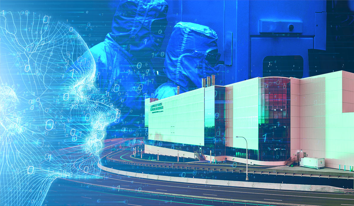
This is why the announcement today of Applied’s new Materials Engineering Technology Accelerator (META Center) is so significant. To be located in Albany, New York, it will be a first-of-its kind R&D facility that brings together the technology ecosystem to accelerate speed of innovation and connectivity to pioneer novel ways to drive advancements in computing. Applied will furnish the META Center with a comprehensive set of our most advanced process systems together with complementary systems needed to bring materials engineering innovations into advanced devices along with systematic data gathering and analysis.
Our goal for the META Center is to rapidly advance the availability of next-generation devices, both in traditional semiconductors and in adjacent and new markets. Part of the solution for achieving this is to bring the entire strength of Applied Materials and its ability to develop and use the broadest set of materials and new combinations of materials to engineer new devices. The world-class center will provide the most optimized materials engineering capabilities to enhance collaboration and R&D across the ecosystem — from materials to systems.
The META Center is unique as an R&D facility by being primarily set up for materials innovations and accelerating related process technologies for high-volume manufacturing by our customers. With the facility, we are addressing the growing need of chip manufacturers and ecosystem partners for access to a leading-edge development environment focused on enabling breakthroughs in novel materials and structures.
Let’s take a look at several areas that represent the kinds of collaboration we would like to foster at the META Center. Examples include our on-going R&D work for new materials-enabled non-volatile memory technology and the development of a new type of electronic switch for AI that mimics the way the human brain works.
When the META Center becomes fully operational next year, we can expand on such collaborative research to improve the cycle time for running pilot structures and production concepts for much quicker learning cycles. The center will help enable advanced process development by offering a fixed process where projects can be run repeatedly to focus not only on performance and reliability data but also on manufacturability.
The META Center is a strategic addition to Applied’s global R&D environment. It complements and builds on the capabilities of the Maydan Technology Center (MTC) in Silicon Valley, which will continue to focus on process system development. The META Center will also support startups and emerging technology companies in fields such as AI, augmented and virtual reality (AR/VR), advanced optics, Big Data, life sciences, autonomous vehicles and more.
Combined, the META Center and MTC will represent an unparalleled concentration of materials innovation made available by Applied Materials in the spirit of fueling the growth of the industries we serve, from materials to systems.
Finally, Applied’s strong commitment will be further supported by a new co-investment initiative between Applied’s venture capital arm, Applied Ventures, LLC, and Empire State Development, the economic development organization of New York. The goal is to invest in promising startups in Upstate New York across a broad range of both established and emerging industries. The materials engineering capabilities of the META Center can solve challenges and drive roadmaps in industries beyond semiconductors. With private sector companies, universities and government working together, we can achieve the knowledge and momentum to fuel a new era of technology.
Tags: r&d, Semiconductors, AI, artificial intelligence, materials engineering, new memory
Mike Chudzik, Ph.D.
Vice President, Technology

Dr. Chudzik is a Vice President of Technology at Applied Materials. He manages teams of device integrators, process and device engineers and program managers to execute on large scale device fabrication projects. Prior to Applied Materials, Mike was at IBM for 14 years where he led teams in the R&D of advanced semiconductor process integration. He received his Ph.D. in electrical engineering at Northwestern University.

Now is the Time for Flat Optics
For many centuries, optical technologies have utilized the same principles and components to bend and manipulate light. Now, another strategy to control light—metasurface optics or flat optics—is moving out of academic labs and heading toward commercial viability.

Seeing a Bright Future for Flat Optics
We are at the beginning of a new technological era for the field of optics. To accelerate the commercialization of Flat Optics, a larger collaborative effort is needed to scale the technology and deliver its full benefits to a wide range of applications.

Introducing Breakthroughs in Materials Engineering for DRAM Scaling
To help the industry meet global demand for more affordable, high-performance memory, Applied Materials today introduced solutions that support three levers of DRAM scaling.