Products & Technologies
Products & Services
Contact
Products & Services
Products & Technologies
Services
Resources
Contact
Posted
October 24, 2023

Stay updated on our content.
Q&A: Galvanizing the Ecosystem to Drive Innovation in Compound Semiconductors

by Applied Blog
October 24, 2023
While silicon-based semiconductors made possible the modern electronics industry, compound semiconductors are poised to deliver a new wave of advances, from 5G communications to autonomous electric vehicles. Composed of chemical elements belonging to two or more different groups in the periodic table, compound semiconductors have unique material properties that enable high-speed and high-power devices that operate at higher voltages and consume a fraction of the energy.
To deliver on the tremendous promise of compound semiconductors, a range of manufacturing challenges need to be overcome. Applied Materials recently hosted a Compound Semiconductor Forum in Taiwan with leaders from across the manufacturing ecosystem. Approximately 130 people from more than 20 companies joined the event. We sat down with David Britz, Senior Director of Strategic Marketing for Applied’s ICAPS* Business, to learn more about the event and how Applied is enabling the next era of innovation in this exciting field.
People often assume that innovation is primarily happening at the leading edge of logic. What are the innovation opportunities in the compound semiconductor space?

David Britz
Senior Director of Strategic Marketing for ICAPS
We talk frequently about leading logic as being driven by scaling. In ICAPS, we are dealing with fabs that aren’t going to do the most advanced nodes in terms of feature size. So, what other knobs do we have? Almost all of them are materials engineering knobs.
Scaling alone is not going to drive device performance in the same way that we think about for a leading logic device. The benefits you get are primarily from materials innovations, and those are frequently not as well understood in terms of the types of materials that can work and how you can get reliability in a use case. Take power devices for example. There is a huge amount of materials innovation happening in power devices.
And so, there are all kinds of interesting challenges that really steer back to device and process innovations where Applied Materials can make an impact. For me as a Ph.D. materials scientist, it doesn’t get any more exciting than this!
You mentioned power devices. That’s a good segue to talk about Applied’s recent Compound Semiconductor Forum. Can you explain why we hosted this event?
It was an Applied-hosted event where we invited customers, collaborators and partners in the ecosystem to get together and talk about the state of compound semiconductors. Why did we invite the entire ecosystem and not just customers? We know this is a unique time in the semiconductor world. More so than ever, we have learned that Applied alone can’t enable customer roadmaps. We really need to work across the ecosystem to help our customers. So that was the idea – it was set up around structured presentations, but also a lot of time for people to have breakout discussions, have informal conversations and come up with ideas based on what we heard during the sessions.
Can you talk a little bit about the structure of the ecosystem in compound semiconductors? Many people are familiar with the makeup of the foundry/logic ecosystem. How do they compare?
In some ways, you have similar dynamics to the typical logic structure. You have some IDMs (integrated device manufacturers) and some foundries. But the reason for having IDMs and foundries is a little bit different in the compound semiconductor world.
Take Gallium Nitride (GaN) as an example. If you're building a GaN device on silicon, the substrate is relatively inexpensive, but the whole process stack can be exceptionally complex. You know you will have to go through learning cycles to get a very high-performance, high-yielding device. Something like that can play very well to a foundry for a mass-market application that ends up in a consumer device. On the other hand, there typically aren’t standard libraries of devices that you can build from in the foundry ecosystem, because of the materials being used. So IDMs will frequently do a lot more work on something like a power discrete device, where there's not a lot of design complexity.
In compound semiconductors, both foundries and IDMs serve diverse end markets with a range of volumes – from consumer smartphones to specialized components in satellites. We'll even see examples where companies have in-house manufacturing capability, but they'll also contract out some percentage of their demand to the foundries. It's a very intertwined ecosystem – some of it has to do with technology, some of it has to do with scale, and then some of it comes down to the complexity of the chips themselves.
We keep hearing that there is a lot of demand and growth potential in this space. What are the applications and trends that are driving this demand?
I'd say that the big umbrella demand driver is this profound change that's happening in how electricity is generated, delivered and used. Around the world we’re seeing coal power plants being retired and replaced with renewable energy generation. To deliver power from a turbine to the grid, there's almost no semiconductor content required. It's basically direct alternating current generation that gets fed directly onto the grid. But the situation is different when you have a renewable source. For example, solar is direct current and you need to convert it to alternating current. Wind is alternating current, but you need to get the phase of the alternating current synchronized with the grid, and that power conversion drives a lot of semiconductor content.
We’re also seeing things that were powered by fossil fuels – like internal combustion engine vehicles – shifting over to electric. Instead of going to a gas station to fill up your vehicle, you fill up your battery at a charging station, which has power electronics in it. And then when the battery discharges, it goes through a power conversion. This means you need a power inverter in the vehicle, as well as a whole bunch of other power electronics around it, which never existed in a car before. That whole ecosystem from generation all the way through use is changing in a profound way, which is driving more and more semiconductor content, in particular power devices.
One area that we see growing – especially because of electric vehicles – is silicon carbide (SiC). That's one of the biggest segments, and it’s growing very quickly because it's one of the key components for the main inverter in electric vehicles. But it also factors into the charging infrastructure, which really needs very efficient power semiconductors because of the amount of current that these things are using today.

Transition to electric vehicles with adoption of ADAS increases ICAPS semiconductor content
You've painted a clear picture of the opportunity here, which is why we brought the ecosystem together to talk about this. What were some of the key themes that were highlighted during the forum?
We all see an opportunity to leverage Taiwan’s established foundry ecosystem, where they have a lot of 6-inch and 8-inch fabs. How do we use this existing infrastructure to contribute to this growth wave? Some people are building new fabs, while others are repurposing older fabs by adding new tool capabilities. So that was a big theme: how can you jump into this ecosystem in a way that is cost effective and gives you a good technology capability, while meeting the more stringent quality, reliability and yield requirements that the industry is going to have?
Another big topic of discussion was around GaN. This technology has found a strong niche in consumer markets, in particular, smart chargers for phones and laptops. The question has always been if you can get the reliability of these devices to an acceptable level for an application like automotive. And that's also a key point that I think the industry needs to work out and needs to put a lot of resources in to.
The third key theme was around the pending wafer size transition from 6 to 8 inch, particularly for SiC. One of the key challenges is that there's not a steady supply of 8-inch wafers available. And even if there was, the wafers are still expected to be fairly expensive for some time. So there's this underlying question about when the wafers be available and cost effective. The debate is really about when the transition is going to happen and if there is a window where a 6-inch fab can continue to be cost-competitive in a world where the IDMs have moved to 8 inch.
There are a lot of manufacturing challenges in this space. What is the role Applied can play in addressing these?
If you look around a typical 6-inch or 8-inch fab, there are a lot of Applied Materials tools. On the device side, we’re addressing a pretty significant portion of the overall equipment set that's critical to SiC. Our role is to continue to support customer needs there. We're actively working with customers to make sure that the tools can do what they need – that they're capable and meeting customer requirements.
As a material, SiC is so unique that we need to make sure our tools are solving the SiC-specific problems. CMP* is a good example. We recently launched a new tool called the Mirra® Durum™ CMP system. SiC is one of the hardest materials known to man – polishing it is not easy. Making sure that our tools meet the requirements day-in and day-out requires close collaboration with customers.

Applied’s Mirra® Durum™ CMP system produces uniform SiC wafers with the highest quality surfaces by integrating polishing, materials removal measurement, cleaning and drying in a single system.
*ICAPS = IoT, Communications, Automotive, Power and Sensors
*CMP = Chemical Mechanical Planarization
Applied Materials
Corporate Communications
The Applied Materials team publishes posts of general interest to our readers.

Doubling Down on Collaboration at SEMICON West 2023
The semiconductor industry has proven itself more than capable of achieving growth by collaborating to overcome big challenges. Collectively, we have demonstrated innovation and resiliency that is fueling what several industry analyst firms project will be a $1 trillion semiconductor market by 2030 that could directly seed $3-4 trillion of global electronics growth.
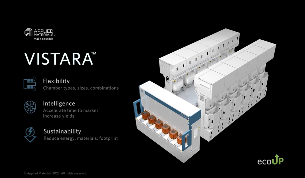
A Deeper Look into the New Vistara™ Platform
Today marks a major milestone in Applied Materials history. At SEMICON West 2023, we introduced Vistara™, a wafer manufacturing platform designed to provide chipmakers with the flexibility, intelligence and sustainability needed to tackle growing chipmaking challenges.

Applied Materials Earns Intel’s 2023 EPIC Outstanding Supplier Award with Supplier Diversity Distinction
Applied Materials has earned the exclusive Intel EPIC Program Outstanding Supplier Award with Supplier Diversity Distinction for 2023. This award recognizes the absolute top performers in the Intel supply chain for their dedication to continuous quality improvement, performance, collaboration and inclusion over the past year.