Products & Technologies
Products & Services
Contact
Posted
February 19, 2025

Stay updated on our content.
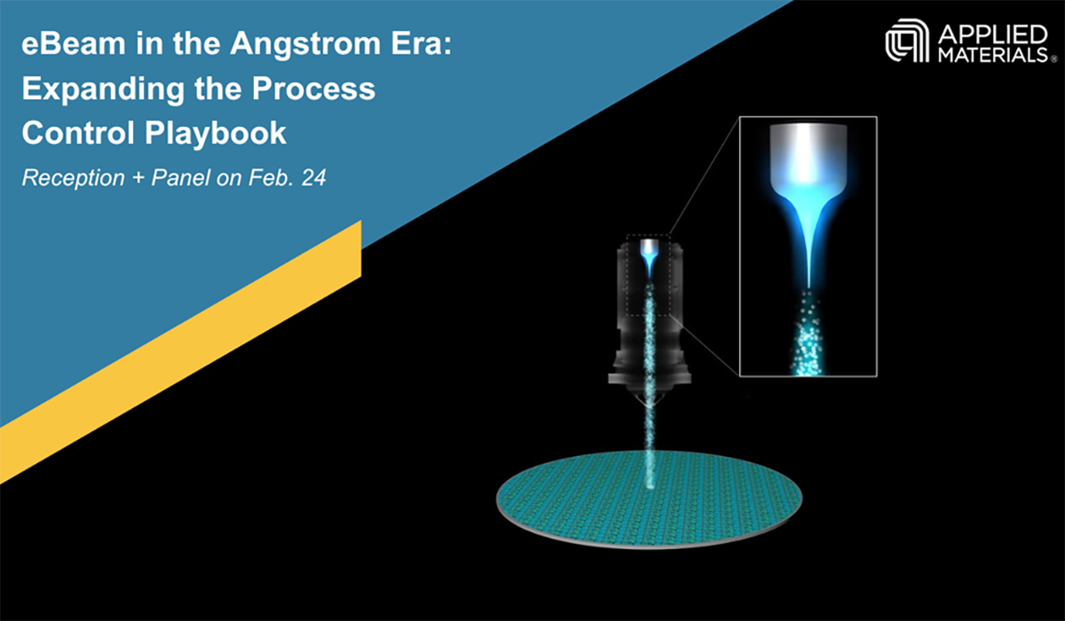
Expert Panel To Explore Advances in eBeam Technology
By Applied Materials Blog
February 19, 2025
What’s New: Alongside the 2025 SPIE Advanced Lithography + Patterning conference in San Jose, CA, Applied Materials will bring together a panel of experts from across the semiconductor ecosystem to explore how chipmakers are increasingly using electron beam (eBeam) technology to continue pushing chip scaling to its limits. The discussion – featuring experts from IBM, imec, Intel and Samsung – will highlight emerging challenges in the “angstrom era” of chipmaking.
More details about the panel can be found on the Applied events page, including a link to register.
Why It Matters: As AI drives demand for advanced logic and memory technologies, the chipmaking roadmap is growing more complex. Critical dimensions continue to shrink, devices adopt new 3D architectures, new chip packaging schemes emerge, and the industry prepares for the transition to High-NA EUV. Each of these opens the door to a growing number of defects that can dramatically impact chip performance and yield. Advancements in process control are becoming more critical to enabling faster and more accurate inspection results.
Who’s Involved: The panel will be moderated by Ofer Adan, Head of Technical Collaborations and Strategic Business Development in Applied’s Imaging and Process Control group, and will feature leading industry experts including:
- Kale Beckwitt, Principal Engineer in Yield, Intel Foundry Technology Development
- Gian Francesco Lorusso, Principal Scientist, Inspection, Metrology and Review, imec
- Luciana Meli, Senior Technical Staff Member, Senior Manager for Lithography and Metrology, IBM Research
- Younghoon Sohn, VP of Technology, Memory Metrology and Inspection Technology, Samsung
Digging Deeper: eBeam imaging has long been an important tool for examining defects that are too small to be seen with optical techniques. Its ultra-high resolution enables detection of the tiniest imperfections in a sea of billions of nanoscale circuit patterns. Traditionally, optical techniques have been used to find defects, while eBeam is deployed to better characterize these defects. In the emerging angstrom era, chipmakers are increasingly taking advantage of eBeam’s superior resolution to identify killer defects buried deep in 3D device structures. At the same time, eBeam plays a growing role in patterning control – enabling the intricate EUV circuit patterns to be placed correctly across a multitude of process steps and layers.
Applied’s expert panel will explore novel eBeam technologies that deliver better and faster imaging of buried nanoscale defects, emerging use cases for eBeam in both process development and high-volume manufacturing, the role of eBeam in new areas such as high-bandwidth memory and advanced packaging, and how eBeam can enable the transistor roadmap as chipmakers develop next-generation architectures such as forksheets and CFETs.
Applied Materials
Corporate Communications
The Applied Materials team publishes posts of general interest to our readers.

Advanced Packaging Enters a New Dimension
For more than a decade, Applied Materials has hosted a technical program alongside the IEEE International Electron Devices Meeting (IEDM) – the premier conference on leading-edge semiconductor technology. For this year’s program, we brought together some of the industry’s brightest minds to discuss the future of chip packaging in the AI era.
Celebrating 30 Years of Display Innovation
This month, Applied celebrated 30 years of innovation in display equipment. We have a long heritage of leveraging technologies developed for semiconductor manufacturing to help drive key display inflections, and we are well positioned to lead again in the next major inflection, which is bringing the superior OLED display technology found in high-end smartphones to millions more devices, ranging from AR/VR headsets to tablets, PCs and TVs.
Bringing eBeam Review to Compound Semiconductors
The power electronics industry has seen a resurgence in the past two decades – driven first by the advent of specialized power management chips for smartphones and tablets, and more recently by the major global transition to renewable energy sources and electric vehicles.