Products & Technologies

Products & Services
Company
Contact
Back to Menu
Products & Services
Products & Technologies
Services
Resources
Company
Contact
Posted
October 01, 2018

Stay updated on our content.
Enabling AI Designs: Where Does the Next Big Innovation Need to Come From?
Oct 01, 2018
Never has there been more demand for “The Big Innovation” — one that moves the needle for performance, power and area-cost (PPAC) in a big way — as there is in the current era of AI and machine learning (ML). As summarized in Why AI Workloads Require New Computing Architectures AI workloads require new architectures to process data. These workloads also call for heterogeneous compute and integration schemes, which stress different PPAC figures of merit.
There is broad consensus that AI is one of the most exciting and pervasive inflections to happen in our lifetime. While many innovations helped solve challenges during the PC and mobile eras, AI is challenging the entire design ecosystem — from materials to systems — in a way that we haven’t experienced before.
At the same time, the performance benefits from the almost linear Dennard and Moore’s Law scaling have slowed down. The two-year cycle for new technology nodes is no longer happening. Further, the economics of transitioning to newer technology nodes is becoming prohibitive for all but a few chip makers. However, the thrust on AI, ML and deep learning (DL) development continues at a furious pace.
My focus here is not the slowdown of Moore’s Law, but rather that innovations will continue to meet the compute demands of these new workloads. As before, when at seemingly impossible crossroads, an innovation has always saved the day. For example, when gate oxide thickness became a barrier to scaling, high-k metal gate technology came along. Or when patterning or photolithography hit a wall, double and quadruple patterning and EUV became a reality.
Today, on the design and architecture side, innovations continue with faster, more efficient ways to process, move and store data. EDA and IP technologies have grown by leaps and bounds. EDA tools manage to churn larger, faster, more power-efficient designs set to increasingly complex design rules. The growth in IP has been phenomenal, with fabless companies outsourcing larger sizes and greater numbers of IP blocks. IP vendors continue to provide silicon-proven IP to newer and better versions of protocol specifications at a faster pace and at newer technology nodes.
The question is: will these individual advances in architecture, design, EDA, IP, technology and heterogeneous integration schemes adequately meet the requirements of new AI compute workloads? And, will there be enough of these individual advances to meet the rising number of new design challenges? Will the innovations accelerate to match the pace of demand for the new workloads or will necessity force the next big invention, a fundamental one that will move the needle in a big way? If so, where will that come from?
Regardless of how we get there, I believe the following:
- Innovations in materials engineering and in materials integration are essential parts of the solution
- Innovations in architecture, design, EDA, IP, technology and heterogeneous integration schemes must continue at their current furious pace
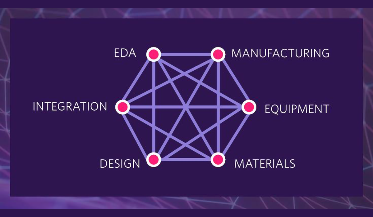
- The most important part of the solution is accelerating connectivity through the tiers listed in #2
As my colleague pointed out in a recent blog, advanced technology nodes require novel materials that are enabled by Integrated Materials Solutions. For example, current materials used for the contact and lower interconnects create a bottleneck to transistor performance at the foundry 7nm and below technology nodes because they are difficult to scale due to the total thickness of the required liners, barriers and adhesion layers. Novel materials and material integration schemes are required for advanced nodes but also for new memories such as RRAM and MRAM.
EDA challenges continue with the requirement to be ready with design tools, reference flows and IP for the newest technology. With the increasing functional complexity of chips, fabless companies are using larger blocks of IP. However, given the escalating costs of designs at newer nodes, many companies are opting to design to more mature nodes. The onus of verifying and qualifying feature-rich IP at newer and older nodes is on the IP provider. Heterogeneous integration schemes using 3D packaging and multi-chip modules (MCM) are seeing newer applications with diversified solutions for logic and memory.
However, none of these advances is the single lever that will enable AI designs. Rather, the key is better and faster connectivity from materials to systems (see figure below).
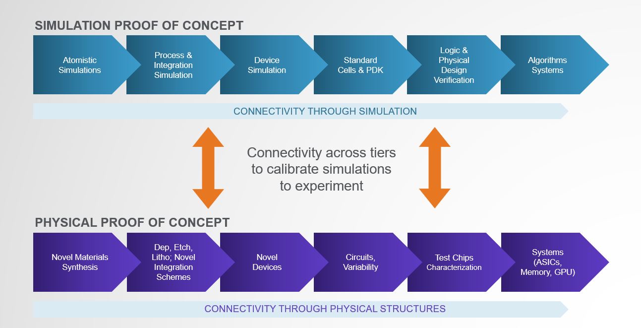
The concept of Design Technology Co-Optimization or DTCO has existed for many years. What is different now is the need for rapid learning cycles from integrating new materials that will turn the required PPAC knob or make possible the end structure for a new memory such as RRAM or MRAM. This requires better connectivity through the different simulation layers, faster material screening and tight calibration between the simulation and physical proof of concept tiers.
In summary, no single knob is going to unlock the productivity gains in the ecosystem to enable AI designs. Rather it is a combination of innovations in new materials, devices and memories; but most importantly, it requires accelerating the connectivity through the different tiers from materials to systems.
Tags: artificial intelligence, AI, machine learning, EDA, nodes, materials engineeriing
Buvna Ayyagari-Sangamalli
Head of Design Technology

Buvna Ayyagari-Sangamalli heads the Design Technology team at Applied Materials. With a career in various roles from Design Engineering to development of Customer IP Subsystems, she is intimately familiar with design challenges. At Synopsys she played a pivotal role in growing the IP business, where she led the IP Applications Engineering team and launched Customer IP Subsystems for AI, Automotive, IoT and other segments. Prior to that, she played a critical role in defining low-power EDA design methodologies. At Intel she worked on various mobile, desktop and processor chips. Her well-rounded 20 years in the semiconductor industry straddled architecture, design, EDA and IP.

Now is the Time for Flat Optics
For many centuries, optical technologies have utilized the same principles and components to bend and manipulate light. Now, another strategy to control light—metasurface optics or flat optics—is moving out of academic labs and heading toward commercial viability.

Seeing a Bright Future for Flat Optics
We are at the beginning of a new technological era for the field of optics. To accelerate the commercialization of Flat Optics, a larger collaborative effort is needed to scale the technology and deliver its full benefits to a wide range of applications.

Introducing Breakthroughs in Materials Engineering for DRAM Scaling
To help the industry meet global demand for more affordable, high-performance memory, Applied Materials today introduced solutions that support three levers of DRAM scaling.