Products & Technologies
Products & Services
Contact
Products & Services
Products & Technologies
Services
Resources
Contact
Posted
April 27, 2021

Stay updated on our content.
DRAM Scaling Requires New Materials Engineering Solutions

Apr 27, 2021
Demand for lower-cost, higher-density DRAM has never been greater as the Internet of Things (IoT), autonomous vehicles and 5G connectivity add more devices and exponentially increase data, further straining the edge and cloud computing infrastructure. IoT devices are estimated to total 500 billion by 2030 and generate a yottabyte of data per year—that’s ten to the power of 24 bytes.
The value of data comes from processing it, increasingly by using AI to derive actionable insights. This requires affordable, high-performance DRAM, and lots of it. DRAM makers are racing to overcome a number of physical limitations that, if left unresolved, will impede DRAM performance, power, area and cost. This blog will examine the challenges and opportunities of further scaling capacitors and periphery circuitry.
Each DRAM memory cell is made up of a transistor and a capacitor which need to scale together to enable bit density to increase. Capacitors store charges using a metal-insulator-metal architecture. A deep hole is lined with a thin-metal bottom electrode, typically made of titanium nitride. Then, a thin layer of high-k insulating dielectric material is deposited. Finally, a second metal electrode is deposited (see Figure 1).
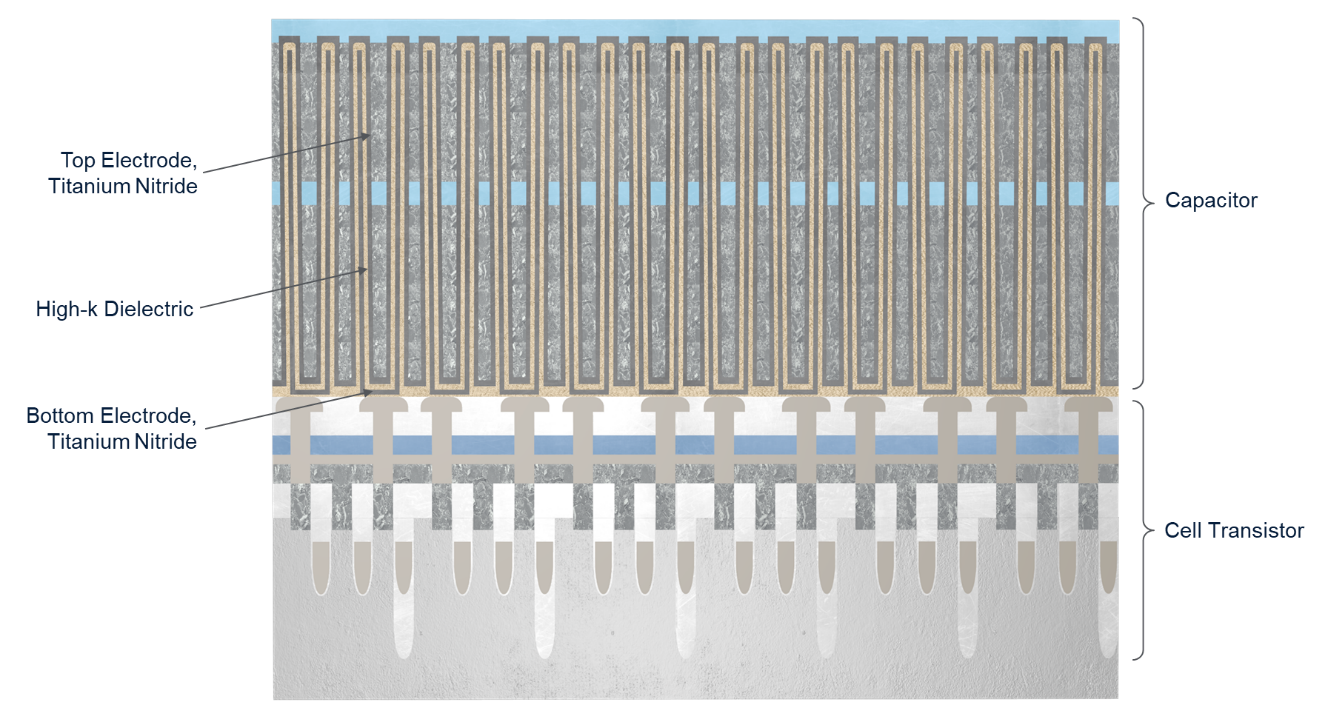
Figure 1: Schematic of DRAM showing an array of transistors (bottom) and tall capacitors (top).
Capacitor Aspect Ratio Scaling
The storage capacitor’s charge is proportional to the surface area of the inside and outside surfaces of the deep hole. The ratio of the hole’s height to its diameter is the aspect ratio. 2D scaling of the memory cells causes the diameter to shrink and, to maintain adequate surface area and charge, the aspect ratio must increase. To continue 2D scaling, chipmakers keep squeezing the capacitor diameter, which pushes the aspect ratio to the extreme.
While a practical idea, the approach is hitting the physical limits of conventional patterning techniques. Specifically, the capacitor holes are defined with sacrificial hard masks made of amorphous polysilicon which are etched through, creating a stencil for a subsequent etch into thick molds that create the increasingly narrow capacitor holes.
As high-energy ions etch the capacitor holes, they also eat away at the hard mask. The higher the aspect ratio, the greater the risk that the hard mask is eroded before the capacitor hole is fully formed, which ruins the chip.
One approach to mitigating this risk has been increasing hard mask thickness, but this also creates issues. The aspect ratio of the taller hard mask plus the narrower capacitor hole combined makes it increasingly difficult to complete the etch and remove all of the etch byproducts. These byproducts can cause twisting, bending, under-etching and other physical defects (see Figure 2).
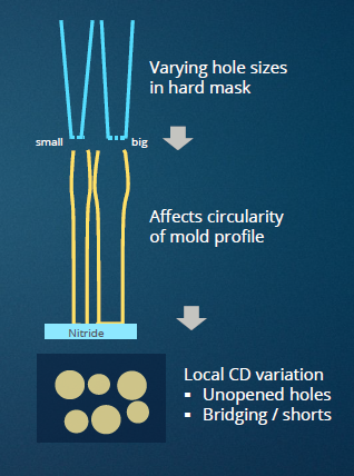
Figure 2: Schematic of typical challenges to scaling DRAM capacitors.
What DRAM makers really need in order to continue scaling is a denser, harder mask material that erodes at a substantially slower rate than the underlying capacitor mold. This thinner hard mask would allow deeper etches along with byproduct removal for perfectly cylindrical and straight capacitor holes with evenly matched depths.
Periphery Circuitry Scaling
A second opportunity to continue DRAM shrinking is to reduce the size of the peripheral circuitry area which consists of the logic transistors and interconnect wiring that surrounds the DRAM cell array (see Figure 3). If the memory cells scale but the periphery circuitry doesn’t, then the periphery takes up an increasing percentage of the die size. The logic is important: it helps determine the performance and power consumption of today’s high-speed DDR4 and emerging DDR5 DRAMs. Each of the metal lines that connect the logic transistors to the cell areas needs to be surrounded by an insulating dielectric material to prevent interference between electrical signals, and the thickness of this dielectric is another key factor impacting scaling. For the past 25 years, DRAM makers have used one of two silicon oxides—silane and tetraethoxysilane (TEOS)—as the dielectric material.
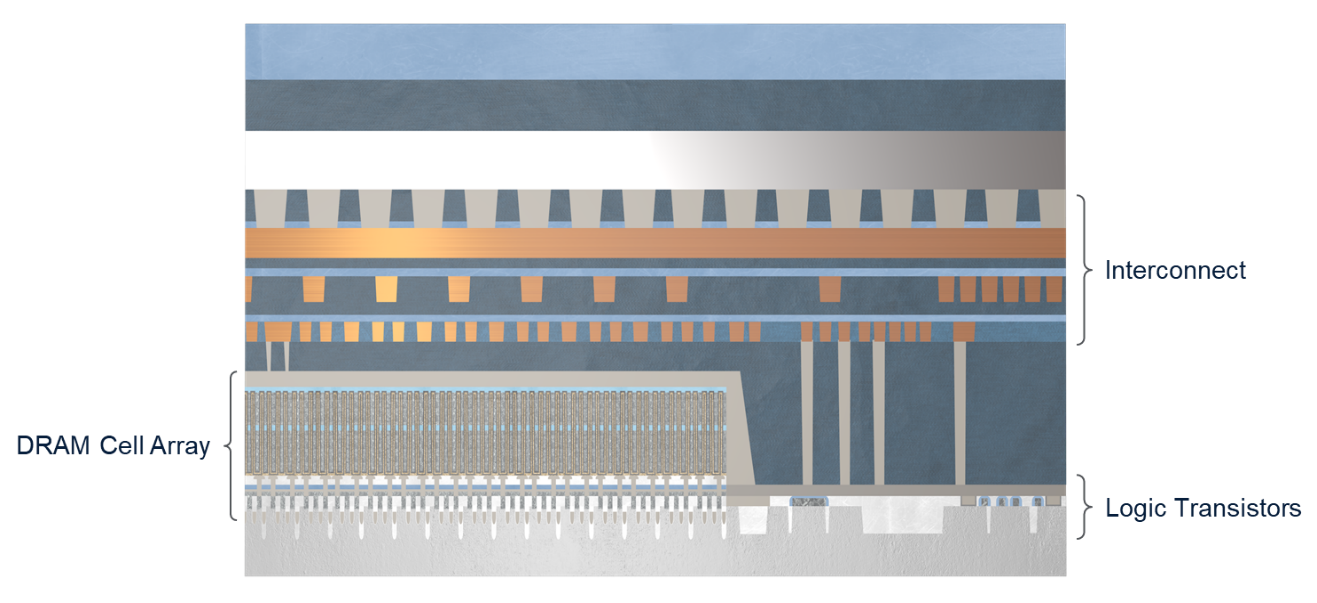
Figure 3: Schematic of DRAM cell array, peripheral logic transistors and interconnect wiring.
Today, DRAM makers are facing the same dielectric scaling challenges faced by leading-edge logic makers around 20 years ago. Beyond a certain point, thinning the dielectrics brings the metal lines so close together that capacitive coupling increases. As a result, the device suffers from increased power consumption, reduced performance, excess heat and potential reliability issues. In logic scaling, the solution was new copper low-k interconnects. In DRAM, the time for a new material that allows metal lines to be placed closer together without causing signal interference is now.
New Materials Research
These DRAM scaling materials engineering challenges—involving patterning hard masks and insulating dielectrics—have been the subject of intense research. In my next blog, I’ll discuss new materials that Applied Materials has been developing to help DRAM makers extend their product roadmaps to meet the world’s growing need for affordable, high-performance DRAMs.
Tags: DRAM, scaling, PPACt, interconnect, hard mask, etch, new ways to shrink
Sony Varghese
Director, Strategic Marketing

Dr. Sony Varghese is director of strategic marketing for memory in the Semiconductor Products Group at Applied Materials. In this role, he is involved in identifying challenges to future key inflections in the memory industry. Prior to Applied Materials, he worked on developing various memory technologies within the R&D organization at Micron Technologies. Dr. Varghese has over 20 U.S. patents issued or pending in the area of semiconductor processing and integration. He holds a master’s degree in materials engineering from The National Institute of Technology Surathkal in India and a Ph.D. in mechanical and materials engineering from Oklahoma State University.

Now is the Time for Flat Optics
For many centuries, optical technologies have utilized the same principles and components to bend and manipulate light. Now, another strategy to control light—metasurface optics or flat optics—is moving out of academic labs and heading toward commercial viability.

Seeing a Bright Future for Flat Optics
We are at the beginning of a new technological era for the field of optics. To accelerate the commercialization of Flat Optics, a larger collaborative effort is needed to scale the technology and deliver its full benefits to a wide range of applications.

Introducing Breakthroughs in Materials Engineering for DRAM Scaling
To help the industry meet global demand for more affordable, high-performance memory, Applied Materials today introduced solutions that support three levers of DRAM scaling.