Products & Technologies
Products & Services
Contact
Back to Menu
Products & Services
Products & Technologies
Services
Resources
Contact
Posted
April 04, 2021

Stay updated on our content.
Display Technology: The OLED Wave and Other Exciting Trends
by Max McDaniel
Apr 04, 2021
In the early 1990s, the modern display industry emerged with the adoption of LCD technology in laptop computers. LCDs provided a thin form factor and a portability that was impossible with the incumbent CRT technology. Over the next 20 years, LCDs diffused beyond laptops and niche devices to dominate the display landscape, displacing CRT in TVs and monitors and enabling new devices such as smartphones. We are now at the start of the next technology replacement wave as OLED displays are emerging to replace LCDs in consumer devices. There are other interesting technologies forthcoming, including mini-LEDs, micro-LEDs and micro-OLEDs. While these names sound similar and are easy to confuse, these are very distinct technologies with different strengths, challenges, applications and time horizons.
The OLED Wave
With their brilliant image quality—high contrast ratio and wide color range—and dynamic form factors including flexible and foldable, OLEDs are already seeing wide adoption in smartphones (~40% penetration this year and increasing fast). Adoption in large-area devices like laptops, tablets and monitors will also grow over the next few years.
This “OLED wave” is transforming the display industry. Already today, all new smartphone fabs are OLED lines, and we will soon see large-area fab investments in OLED. This is good news for companies like Applied Materials because the equipment capex per fab is significantly higher for OLED than for LCDs.
We believe the OLED transition will be a towering technology wave disrupting the vast display ocean over the next decade (see Figure 1).
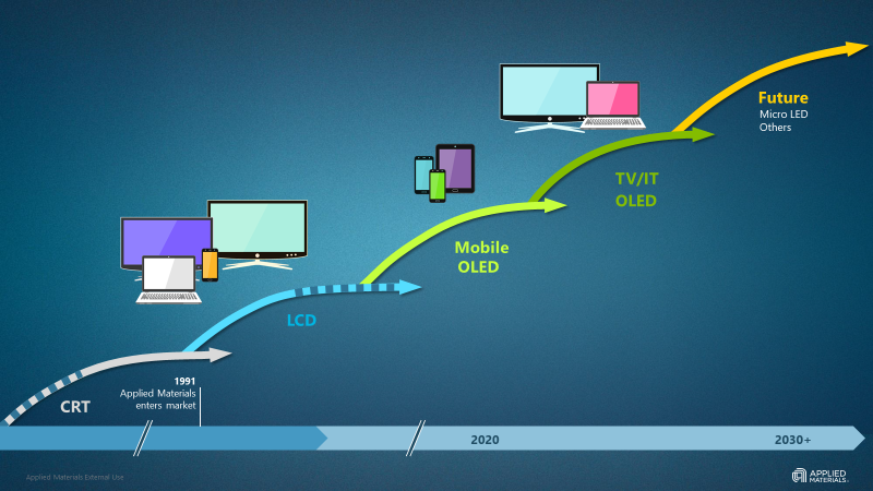
Figure 1: Technology waves in the display industry.
Mini-LED
Mini-LED is an LCD enhancement technology and part of the ongoing effort by LCD makers to narrow the performance gap between LCD and OLED. Mini-LED LCDs employ arrays of very small LEDs (100-1,000 micron size range) in the backlight, behind the LCD panel, to provide more control of pixel illumination (see Figure 2). Mini-LED backlights provide better dark/light contrast versus traditional LCDs by taking advantage of local dimming of multiple zones; this partially narrows the contrast performance gap relative to OLEDs. The challenge with Mini-LED technology comes down to a cost/benefit tradeoff. To get anywhere close to the contrast ratio of OLED, mini-LED LCDs need more than 10,000 individual chips and an active matrix backplane to drive a high-performance backlight. This backlight backplane is needed in addition to the primary backplane already used to drive the LCD pixels. The result is a display that looks better than traditional LCD but not as good as OLED—with a cost that’s at least as high as OLED today. Mini-LED LCDs retain the other deficits versus OLED—a lower color range, slower response times and a thicker form factor.
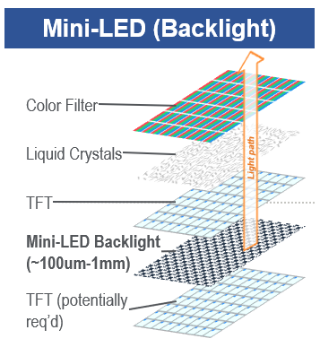
Figure 2: Mini-LED LCDs employ very small LEDs in the backlight, placed in an array behind the LCD panel to provide illumination for the pixels.
Micro-LED
Whereas mini-LED is just an LCD backlight enhancement, micro-LED is a self-emitting display technology (like OLED) using LEDs less than 50-100 microns in size, each becoming an individual red, green or blue sub-pixel (see Figure 3). Micro-LED technology matches or exceeds OLED and LCD in almost every performance area. It has the image quality and form factor benefits of OLED without the robustness and lifetime issues. It exceeds LCD and OLED in terms of brightness and also has lower power consumption. Micro-LED is indeed the “holy grail” of displays.
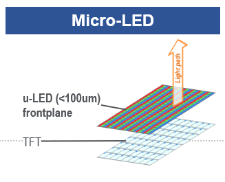
Figure 3: Micro-LED is a self-emitting display technology using LEDs less than 100 microns in size, placed directly in each pixel.
But there is a catch—actually two, related catches—manufacturability and cost. One example of the manufacturing challenges is the pick-and-place step. Placing each individual micro-LED into the pixel areas is difficult. In a 4K display there are ~24 million sub-pixels and 8K displays use ~100 million. So, to make a micro-LED display, tens of millions of sub-micron LEDs must be removed from the substrate they are produced on and precisely placed in their designated sub pixel with good electrical contact. This “pick and place” manufacturing step is fraught with yield risks. It’s as delicate as using robotic machinery to handle pollen. There are many pick and place technologies under development today, but none yet meet the productivity and yield requirements of manufacturing mainstream consumer displays. And then there is the cost issue. Due to the manufacturability problems plus the fundamental high cost of millions of LED chips, the cost of micro-LED displays remains far too high for mainstream applications. To illustrate this, we know that the micro-LED TVs for sale today are priced well above $100K dollars. A cost reduction of more than 100x is needed to reach even the very high-end consumer TV market.
Because of these cost and manufacturability challenges, we expect micro-LED to be limited to niche applications, such as augmented reality (AR), wearables and extreme high-end public information displays, for the next several years at least. But with innovations and improvements, micro-LED might pose a challenge to OLED in the mainstream consumer applications after 2030. I can’t wait!
Micro-OLED
Micro-OLED is another interesting technology emerging in displays. It enables very high resolution (greater than 1,000 pixels per inch) and can be used in near-eye applications like virtual and augmented reality (VR/AR). Micro-OLED can be manufactured with a frontplane similar to the White OLED (WOLED) technology used in TVs today (blanket OLED layers are evaporated onto a substrate to emit white color; then a color filter renders the light red, green or blue). But to enable the high resolution and small pixels, the backplane is built on silicon wafers using semiconductor manufacturing technology (see Figure 4). Micro-OLED is a viable technology, but its application is expected to be limited to small, near-eye or projected displays, and we do not expect it to challenge conventional OLED for mainstream applications.
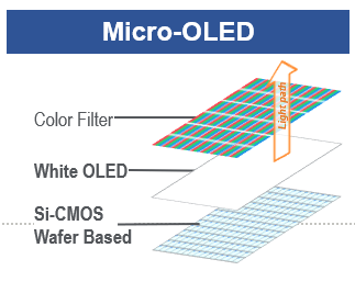
Figure 4: Micro-OLED can be manufactured with a frontplane similar to current White OLED technology used in OLED TVs; to enable the high resolution and small pixels, the backplane is built on silicon wafers.
Summary
LCD has been the dominant display technology for nearly 30 years. The next technology inflection, OLEDs, is upon us and will drive a new wave of fab investments for the next decade. While this will be the dominant inflection, we will see other technologies vying to gain traction as well. For Applied Materials, all of these inflections are positive for our business. OLED roughly doubles the equipment capex per fab versus traditional LCD, significantly increasing our opportunity in both the backplane and the frontplane. Mini-LEDs require a second backplane for the backlight which increases the number of process equipment steps. Micro-LED requires further innovation on die manufacturing and high-end backplanes, which potentially creates significant opportunities for our display and semiconductor technologies on the frontplane. And while targeting a small subset of the market, micro-OLED also provides opportunities for Applied’s display and wafer-based capabilities.
We see a bright future for the display industry over the next decade, with dramatic new technologies on the horizon. Together with our customers, peers and partners, we will create even more dynamic and stunning visual experiences for consumers.
Tags: LCD, OLED, Mini-LED, Micro-LED, Micro-OLED
Max McDaniel
Vice President and Chief Marketing Officer, Display Group

Max McDaniel is the Chief Marketing Officer of Applied Materials Display and Flexible Technology Group. He has held engineering, marketing and financial management roles in high-tech equipment companies for over 25 years. Mr. McDaniel has been at Applied Materials since 2003. Prior to joining Applied Materials he served over twelve years at Watkins-Johnson, a Semiconductor and LCD equipment manufacturer, where he worked in R&D, engineering, and marketing roles.
He holds a Bachelor’s degree in Physics from the University of California, Santa Cruz, and an MBA from Washington University in St. Louis.
Display Trends at CES 2018
There is no place like CES to see the most exciting new and future displays. Beyond traditional technologies like television, displays also featured prominently in many of the big trends at the show: AI, automotive, VR, IoT and connectivity.

Innovations in eBeam Metrology Enable a New Playbook for Patterning Control
The patterning challenges of today’s most advanced logic and memory chips can be solved with a new playbook that takes the industry from optical target-based approximation to actual, on-device measurements; limited statistical sampling to massive, across-wafer sampling; and single-layer patterning control to integrative multi-layer control. Applied’s new PROVision® 3E system is designed to enable this new playbook.

Breakthrough in Metrology Needed for Patterning Advanced Logic and Memory Chips
As the semiconductor industry increasingly moves from simple 2D chip designs to complex 3D designs based on multipatterning and EUV, patterning control has reached an inflection point. The optical overlay tools and techniques the semiconductor industry traditionally used to reduce errors are simply not precise enough for today’s leading-edge logic and memory chips.