Products & Technologies
Products & Services
Contact
Back to Menu
Products & Services
Products & Technologies
Services
Resources
Contact
Posted
December 17, 2018

Stay updated on our content.
Cobalt Enables Power and Performance Scaling at Single-Digit Logic Nodes

Dec 17, 2018
Chip designers require simultaneous improvements in “PPAC”: power, performance and area/cost (Fig. 1). Achieving these improvements is becoming increasingly difficult as classic Moore's Law scaling slows. What's needed is a new playbook for the industry consisting of new materials, new architectures, new 3D structures within the chip, new methods to shrink feature geometries, and advanced packaging techniques. All these areas require major advances in materials engineering. At the recent IEDM conference, I was invited to discuss solutions to the interconnect challenges that threaten to keep logic device power and performance from scaling with area/cost.
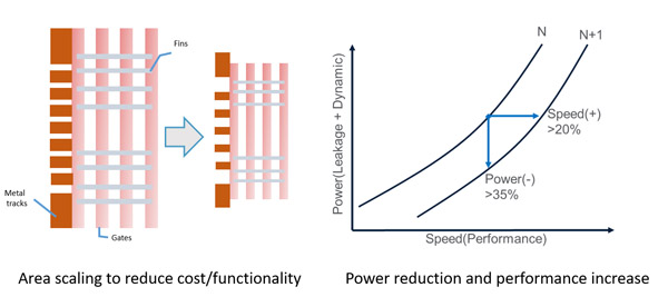
Fig. 1. Logic CMOS scaling goals – performance, power, area and cost improvements.
Transistor Scaling Requires New Materials
The industry has made enormous investments to achieve multiple generations of FinFET scaling. As we enter the single-digit-nanometer regime, however, electrical resistance in the contact and interconnect is negating the area/cost advantages of further transistor scaling.
Specifically, at ever more critical dimensions, tungsten transistor contacts and copper local interconnects are hitting the wall. Continued 2D scaling depends on identifying and successfully integrating new materials that can deliver low power and high performance. Such materials are critical to improving on-current, reducing delay and managing dynamic leakage—enabling power-performance improvements, node after node.
The Promise of Cobalt
Cobalt promises lower resistance at smaller geometries, in part due to the metal’s inherent characteristics when compared to tungsten and copper at small dimensions, and in part because cobalt works with thinner barriers, which allow for sufficient volume to be maintained.
Integrating cobalt is not trivial, but Applied Materials has developed an “Integrated Materials Solution” for cobalt whereby the multiple process chambers needed to integrate cobalt can be combined into the same Endura platform, allowing wafers to be kept in vacuum for pristine materials engineering at ever more critical dimensions.
Reengineering the Transistor Contact and Local Interconnect
Tungsten has been the material of choice for contact metallization due to its ease of integration and reliability. But, we’ve reached the point where it presents a scaling bottleneck. This is because the thickness of the ALD titanium nitride barrier layer that tungsten requires to protect the underlying titanium layer doesn’t scale in proportion with the reduction in critical dimensions (CDs). The result is increased contact resistance and decreased on-state current.
Replacing the tungsten contact and local interconnect with cobalt removes this scaling bottleneck. The interest in cobalt as a new material of choice is driven by the fact that it has bulk resistivity similar to tungsten, yet is about 1.5-2x less resistive due to impurities and grain boundary scattering in tungsten. Other advantages are that CVD cobalt allows a thinner titanium nitride layer and a seamless fill compared to CVD tungsten (Fig. 2).
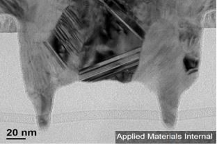
Figure 2. 10nm via structure filled with cobalt shows no seams.
The industry has already begun using cobalt to reduce contact and middle of line resistance. Replacing tungsten contacts with cobalt has paid dividends with an approximate 60 percent improvement in contact line resistance. Replacing the short-length copper interconnect at the lowest metal contact layers with cobalt has reduced via resistance (for lower IR drop) and improved electromigration reliability.[1] To speed customer adoption, Applied has developed a robust Integrated Materials Solution for reliably engineering cobalt contacts and lower-level interconnects.
What is the Future of Copper Interconnects?
Given the advantages of cobalt, the question many ask is why not use it to replace copper in more of the interconnect layers? A detailed analysis of line resistance scaling shows that copper is superior or adequate to CDs of 12-15nm. For metal levels above M1, where the interconnect is long enough for line resistance to be the key performance factor, copper wins.
Copper Extension Continues
There is strong industry incentive to extend copper as far as possible. As discussed, while via resistance is optimized by reducing barrier thickness, line resistance is about maximizing the volume of copper by thinning both the barrier and liner. All of this needs to be accomplished while maintaining perfect metal fill and high reliability.
New, integrated and co-optimized technologies are needed to extend copper (Fig. 3). These include replacing the PVD tantalum nitride barrier with ALD tantalum nitride and using copper reflow on cobalt liners for the fill. The ALD barrier approach provides a path to scale copper below 36nm pitch. Beyond this, selective via fill schemes promise lower via resistance by eliminating high-resistivity barriers, providing new options for addressing interface management issues.
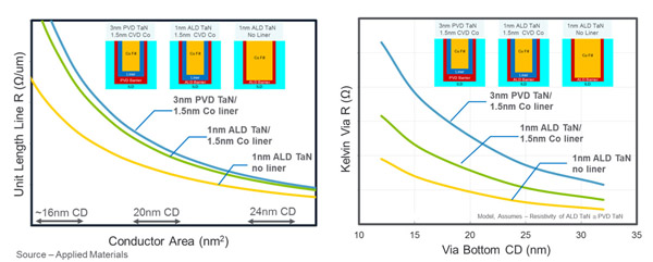
Figure 3. Extending copper requires co-optimization of ALD barriers with thinner liners and new fill technology to maximize conductor volume (low line R) and minimize interface resistance(low via R).
Beyond Copper and Cobalt
Filling smaller interconnects is becoming more difficult, and reliability can suffer. New conductor materials and different metallization schemes and technologies are needed to solve challenges over the long term. The issue goes beyond identifying metals with lower theoretical resistivity: we also need to explore the needs for barriers and liners. We need to determine whether the ever-smaller volumes can be successfully filled, and whether the process can be successfully integrated. The materials engineering challenges include managing the materials interfaces to improve reliability and co-optimizing the barrier-liner-fill to optimize resistance, yield, cost and reliability.
New materials of interest include ruthenium and molybdenum, but both still lag cobalt from a maturity perspective.
Longer Term Solutions
Over the next two to three nodes, the focus will be on extending copper interconnects as long as possible while pioneering the best candidates to eventually replace copper. Looking beyond the horizon, fundamental changes loom. Subtractive etch schemes may help overcome the challenges associated with the damascene approach—but they are in the very early stages of exploration. While promising, such changes represent a seismic shift for the industry, requiring entirely new technology portfolios. As we look to the future of interconnect technology, we foresee numerous issues related to defectivity, yield and reliability issues. Integrated Materials Solutions give us new ways to address etching more exotic metals, filling ever-smaller gaps and self-aligning critical features.
In summary, logic scaling can continue as long as we can also find and successfully integrate promising new materials that allow “PP” to scale with “AC.” The industry needs to accelerate materials innovation, and Applied is delivering Integrated Materials Solutions that can speed customer success.
[1] C. Auth et al, “A 10nm high performance and low power CMOS technology featuring 3rd generation FinFET transistors, self-aligned quad patterning, contact over active gate and cobalt local interconnects,” 2018 IEEE International Electron Devices Meeting (IEDM), San Francisco, CA
Tags: interconnects, Cobalt, copper, contacts, ALD
Mehul Naik, Ph.D.
Master and Vice President of Technology, Semiconductor Products Group

Mehul Naik is a Master and Vice President of Technology with the Advanced Product Technology Development team in the Semiconductor Products Group at Applied Materials. He is responsible for the Logic Program working on inflection mapping and leading cross-functional programs in the FEOL, MEOL and Interconnect area. He has authored over 64 publications and holds over 90 U.S patents. Mehul earned his Ph.D. in chemical engineering from Rensselaer Polytechnic University.

Adding Sustainability to the Definition of Fab Performance
To enable a more sustainable semiconductor industry, new fabs must be designed to maximize output while reducing energy consumption and emissions. In this blog post, I examine Applied Materials’ efforts to drive fab sustainability through the process equipment we develop for chipmakers. It all starts with an evolution in the mindset of how these systems are designed.

Innovations in eBeam Metrology Enable a New Playbook for Patterning Control
The patterning challenges of today’s most advanced logic and memory chips can be solved with a new playbook that takes the industry from optical target-based approximation to actual, on-device measurements; limited statistical sampling to massive, across-wafer sampling; and single-layer patterning control to integrative multi-layer control. Applied’s new PROVision® 3E system is designed to enable this new playbook.

Breakthrough in Metrology Needed for Patterning Advanced Logic and Memory Chips
As the semiconductor industry increasingly moves from simple 2D chip designs to complex 3D designs based on multipatterning and EUV, patterning control has reached an inflection point. The optical overlay tools and techniques the semiconductor industry traditionally used to reduce errors are simply not precise enough for today’s leading-edge logic and memory chips.