Products & Technologies
Products & Services
Contact
Products & Services
Products & Technologies
Services
Resources
Contact
Posted
July 25, 2023

Stay updated on our content.
At SEMICON West, Chip Industry Thought Leaders Rally Around Heterogeneous Integration

by Vincent DiCaprio
July 25, 2023
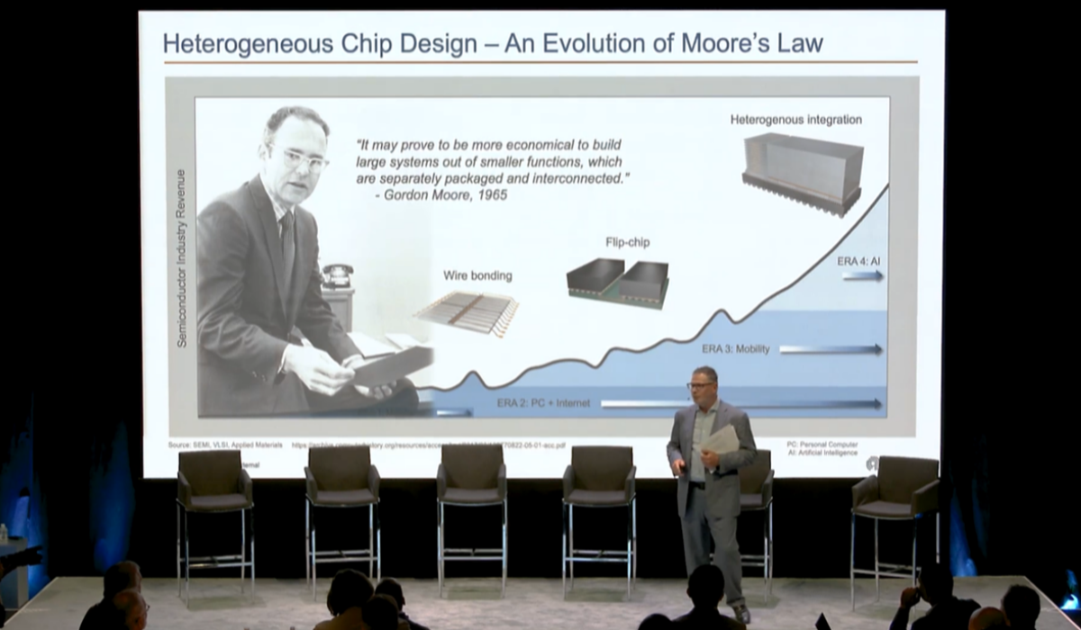
Earlier this month, I had the privilege of moderating a dynamic panel discussion at a well-attended SEMICON West Technology Breakfast hosted by Applied Materials. For several years now, the industry has been buzzing about emerging trends in heterogeneous integration (HI). We wanted to separate the hype from the reality, so we brought together chip design and manufacturing thought leaders from AMD, Intel and Qualcomm – along with leading hybrid bonding solution providers Besi and EV Group.

During the wide-ranging discussion, we looked at the journey each company is taking to enable the evolution of 2D to emerging 3D designs. The panelists explained why HI is increasingly enabling and critical to improvements in system performance, power efficiency, form factor and time-to-market. We discussed the need for collaborative innovation to fully realize the promise of hybrid bonding as well as achieve breakthroughs in advanced substrates and optical technologies that can fuel the roadmap well into the future.
A video replay of the panel is available on our SEMICON West event web page. Below is a brief summary of my key takeaways from the conversation.
A Marriage of Memory and Logic
AMD’s Mark Fuselier noted that a decade ago, the company was already looking at how to reduce cost by building SoCs with small chiplets that were reassembled in package. As AMD progressed this capability, it next used chiplets to bring memory much closer to logic which inspired the adoption of a hybrid bonding technique that pulls SRAM immediately adjacent to the CPU using 3D stacking. Fuselier said AMD’s third-generation effort will enable more advanced HI combining CPU or GPU chiplets with onboard memory specific to each compute workload.
Chidi Chidambaram remarked that increases in complexity make the roadmap less predictable. “Five years ago, I knew that gate-all-around [transistors] would be the technology of 2022,” he said. “But five years from now, I'm not sure what we're going to do.”
Chidambaram posited that heterogeneous integration will become more important than conventional scaling in delivering cellular chipsets that deliver the continually improving user experience people have come to expect. “If you look at the system as a whole, you have RF, power management and memory,” he said. “To get from 5G to 6G, you need the power amplifier performance to come very close to the rest of the system chips. Heterogeneous integration is the key to bringing all this together.”
Intel’s Babak Sabi envisioned a future where compute platforms will be built on what he called “a sea of cores,” with co-located memory driving down latency and increasing bandwidth. Sabi observed that, because advanced packaging is enabled by interconnect wiring density, it will require techniques such as hybrid bonding to enable effective chip stacking – or what he termed “vertical interconnection.” “To be able to do that, you're going to need innovation in wafer-level assembly, because in the AI world, we're talking about huge complexes and the wafer-level integration of whole products,” Sabi said.
Intel believes the adoption of glass substrates will allow the industry to put large wafer complexes together by eliminating the interposer and directly connecting chips. He also expects that, by as soon as the end of the decade, optical interconnects will begin to replace copper wiring in high-speed communications. “If you look further into the future, you're going to replace your electrical mesh with an optical mesh and conduct day-to-day communication using optics,” Sabi said. “That's going to bring a huge performance increase and power reduction.”
Hybrid Bonding Hurdles
Two semiconductor equipment companies on the panel, Besi and EV Group, discussed the hurdles that must be cleared for hybrid bonding to move into very-high-volume manufacturing.
Besi CEO Richard Blickman said a major issue is placement accuracy as design geometries become ever smaller. Perhaps even more critical, he said, is the “handshake” between assembly interconnects and the front-end, where Besi is in the early stages of attaching chip-level interconnects as either chip-on-wafer or chip-on-chip.
“Imagine how you place all of these different die with the accuracy required in the nanometer space,” he said. “There are many new challenges which will have an impact on how hybrid bonding will find its way into the mainstream. But the advantages are so numerous it's not a question if it will happen, it's more a question of timing.”
Wafer-to-wafer hybrid bonding has also been moving up the adoption curve, used in CMOS image sensors for several years and now gaining momentum in 3D NAND. Paul Lindner said that EV Group is collaborating deeply with industry partners to solve the interdependencies between wafer preparation, CMP and other process steps needed to advance the technology. Eventually, active layers will be transferred from one wafer to another and enable backside processing.
“We have demonstrated, collaboratively, that hybrid bonding technology is scalable deep into the submicron range,” Lindner said. “Obviously, the challenge for us as equipment suppliers is to offer the level of precision and cleanliness that will enable that scaling, but I don't see a path where hybrid bonding goes away. When layer transfer technologies are used in advanced nodes or for new transistor architectures, they will offer tremendous integration density when combined with advanced lithography solutions.”
A Call for Collaboration
In the end, the panelists agreed that cross-discipline collaboration is essential to bringing new HI technologies and techniques such as hybrid bonding into the mainstream.
Intel’s Sabi said hybrid bonding blurs the lines between chip fabrication and package assembly. He cited the partnership between Besi and Applied in co-optimizing a hybrid bonding flow as the kind of collaboration needed to accelerate the path forward. Sabi also commented on Applied’s newly announced Equipment and Process Innovation and Commercialization (EPIC) Center. “This is a great move by Applied, bringing everybody from industry, universities, et cetera, together,” he said. “Today, as we do early pathfinding, research and development, these wafers and packages travel 50,000 or 60,000 miles going from one [research] place to another. You lose a lot of quality and a lot of time. By having a center, we can reduce mileage and improve quality. And as a practical matter, it's going to give us a tremendous speed advantage.”
Vincent DiCaprio
Vice President, Business and Corporate Development
Heterogeneous Integration and ICAPS, Semiconductor Products Group

Vincent leads Corporate and Business Development for the Heterogeneous Integration and ICAPS division at Applied Materials, where he is responsible for forging new strategic alliances and partnerships key to technology advancement for future product solutions. Vincent leads all aspects of critical technology inflections related to heterogenous integration, next generation integration of silicon, volumetric scaling for all key aspects of the technology stack related to system level solutions.
Experienced in all facets of the technology sector, Vincent has over 30 years of outstanding achievement in Technology Development, Operations, Business, Sales and Marketing, having demonstrated success at companies like IBM, Amkor, ASE, TSMC, and GLOBALFOUNDRIES. With a degree in Pure and Applied sciences at Champlain Regional College, and a Bachelor of Engineering degree from Concordia University, Vincent is both the author and co-author of 30+ Patents in the field of advanced semiconductor packaging.

Doubling Down on Collaboration at SEMICON West 2023
The semiconductor industry has proven itself more than capable of achieving growth by collaborating to overcome big challenges. Collectively, we have demonstrated innovation and resiliency that is fueling what several industry analyst firms project will be a $1 trillion semiconductor market by 2030 that could directly seed $3-4 trillion of global electronics growth.

As Chipmakers Assess “Where” to Build New Fabs, the “How” of Semiconductor Innovation Must Remain a Priority
According to Ericsson, there are more than 6.5 billion smartphone users worldwide. I would speculate that very few of them have ever given much thought to what’s inside that phone — a miracle of science, engineering and manufacturing that is arguably one of humankind’s greatest technical accomplishments.

Bringing the Future of Advanced Patterning into Focus at SPIE
This year’s SPIE Advanced Lithography + Patterning conference comes at a time when the semiconductor industry needs new breakthroughs to solve the patterning challenges of continued scaling with EUV lithography which will become more intense with the arrival of High-NA EUV.