Products & Technologies
Back to Menu
Products & Technologies
Services
Resources
Posted
October 31, 2024

Stay updated on our content.
Celebrating 30 Years of Display Innovation

By Max McDaniel
October 31, 2024
While Applied Materials is best known for providing the machines that produce the world’s logic and memory chips, we also have a long history of using our differentiated materials engineering capabilities to solve technology challenges in adjacent end-markets.
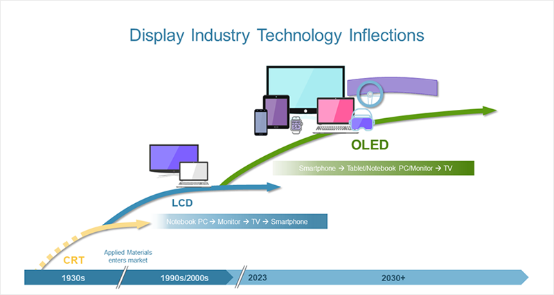
One of the best examples of this approach is our display business. This month, Applied is celebrating 30 years of innovation in display manufacturing equipment. We have a long heritage of developing technologies that have helped drive key display inflections, and we are well positioned to lead again in the next major inflection, which is bringing the superior OLED display technology found in high-end smartphones to millions more devices, ranging from AR/VR headsets to tablets, PCs and TVs.
Leveraging Semiconductor Technologies for Display
Our display journey began in the mid-1990s, when the computer industry sought to replace cathode ray tube (CRT) monitors with a new generation of displays that were thinner, lighter, more durable and energy efficient. At Applied, we realized that some of the semiconductor technologies we designed for making transistors on silicon wafers could be scaled for glass substrates used in manufacturing liquid crystal display (LCD) screens for consumer electronics.
Our first display products were chemical vapor deposition (CVD) systems critical to building the transistors that turn on and off LCD pixels. With our expertise in uniform dielectric deposition, we were able to help the display industry scale the glass substrates through multiple generations of size increases, each time driving down the cost of LCD technology and making it suitable to larger and larger notebook PCs, and eventually desktop monitors and TVs. The LCD revolution had a major impact on TV size growth since CRT technology was limited to around 40 inches. The largest CRT TV ever made – the Sony PVM-4300 – had a 43-inch screen and weighed more than 400 pounds, a far cry from today’s light and thin LCD TVs that commonly approach 100 inches in size.
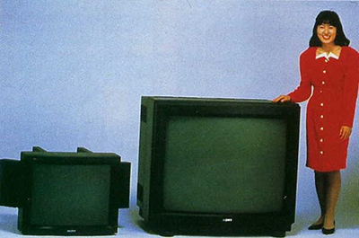
Historical image of the Sony PVM-4300
Along the way we brought our physical vapor deposition (PVD) technology to the display market, using our innovative rotating cathode technology to enable faster and lower-power display transistors. We also adapted our eBeam technology for display manufacturing, allowing our customers to test transistors and non-destructively see and analyze defects within the displays. We enabled in-line review, which improved manufacturing productivity, yield and cost.
Our expertise in both materials engineering and high-volume manufacturing helped our customers create the global LCD display industry, ultimately growing the market to hundreds of millions of units per year. But this was just the beginning.
A second big wave of growth came in the next decade with the mobility revolution. The smartphone market exploded, and device makers began looking for new materials and structures to deliver the higher image resolution needed in these smaller displays along with thinner form factors and lower power for longer battery life. The semiconductor industry is on a constant journey for improvements in chip performance, power, area-cost and time to market (PPACt), so Applied was able to tap our expertise in improving chip transistor and wiring to help enable a new generation of organic light-emitting diode (OLED) displays for high-end smartphones from the world’s leading brands.
First, we helped enable a significant improvement in display performance with a new kind of transistor called low-temperature polysilicon (LTPS). While LTPS manufacturing was more complex than the previous incumbent technique, it enables higher OLED pixel density and thereby resolution. Because OLED materials are fragile, we adapted our CVD technology for OLED thin-film encapsulation, which hermetically seals and protects the OLED films from any exposure to air and moisture.
These technology adaptations helped catalyze OLED adoption in smartphones, the largest-selling consumer electronics product category. The higher materials engineering intensity of OLED displays created a new wave of factory and equipment spending, which added to Applied’s display revenue and helped the company become the world’s largest display equipment manufacturer with leadership positions in its target market segments.
In recent years, while the display industry has been in a correction period, we have continued to invest to solidify our technology leadership and strengthen our core products in CVD, PVD, thin-film encapsulation and eBeam testing and review. We also adopted another concept from our semiconductor business: the Integrated Materials Solution™ approach, where we combine multiple adjacent process steps in a single, high-vacuum system to protect and carefully engineer interfaces between ever-thinner layers of materials. This “fab within a fab” approach is helping our display customers develop new generations of faster transistors that use less power, paving the way for more exciting consumer electronics devices in the years ahead.
Innovating for the Next Wave of Growth
The past 30 years of display innovation was about transitioning from CRT to LCD, scaling up thin displays from the smallest notebook PCs to the largest TVs, and giving high-end smartphones the best display technology of all. Today, the display industry is on the cusp of another major inflection: expanding OLED penetration to the hundreds of millions of tablets, notebook PCs and IT monitors sold each year. Once it becomes practical to scale OLED manufacturing to the larger glass panels used to build these displays, consumers can look forward to brighter displays with wider viewing angles; higher resolution and refresh rates; thinner and even flexible screens; and lower power and longer battery life.
Bringing OLED technology to these IT devices represents a massive opportunity for the display industry since the number of LCD units sold each year multiplied by the larger screen area of these devices represents a display area opportunity several times larger than smartphones.
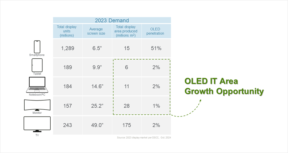
Accelerating OLED adoption in these end markets could require billions of dollars in new fab equipment spending. Converting the TV market to OLED technology would require another massive investment in new display manufacturing capacity and many years of high-volume production.
As we embark on the next 30 years of our journey, Applied is focusing on new ways to use our materials engineering and high-volume manufacturing know-how to bring more exciting innovations to the display industry, which will be even more dynamic in the decades ahead.
Max McDaniel
Vice President and Chief Marketing Officer, Display Group

Max McDaniel is the Chief Marketing Officer of Applied Materials Display and Flexible Technology Group. He has held engineering, marketing and financial management roles in high-tech equipment companies for over 25 years. Mr. McDaniel has been at Applied Materials since 2003. Prior to joining Applied Materials he served over twelve years at Watkins-Johnson, a Semiconductor and LCD equipment manufacturer, where he worked in R&D, engineering, and marketing roles.
He holds a Bachelor’s degree in Physics from the University of California, Santa Cruz, and an MBA from Washington University in St. Louis.
Bringing eBeam Review to Compound Semiconductors
The power electronics industry has seen a resurgence in the past two decades – driven first by the advent of specialized power management chips for smartphones and tablets, and more recently by the major global transition to renewable energy sources and electric vehicles.

Implant Innovation Enables the Compound Semiconductor Roadmap
AI may have taken center stage among the drivers for chip industry growth, but there is another global inflection fueling the semiconductor roadmap: the clean energy revolution. Featuring major structural shifts to renewable energy sources, smart grid technologies and electric vehicles, the star player in clean energy is the power semiconductor, which controls and converts electrical energy to supply power for a wide variety of electronic devices.
Understanding the Inflection in Wafer Fab Equipment Growth
In my previous blog, I outlined a framework for why we at Applied Materials believe the wafer fab equipment (WFE) market can grow as fast or faster than the broader semiconductor industry.
