Products & Technologies
Products & Services
Contact
Back to Menu
Products & Services
Products & Technologies
Services
Resources
Contact
Blog Archive

Optical Circuit Switches Show Promise for More Energy-Efficient AI Data Centers
Applied Ventures is actively investing in photonics startups to foster a vibrant ecosystem to build high-speed, energy-efficient networks for next-generation data centers. While traditional electrical packet switches are approaching their technical limits, optical circuit switches offer a particularly promising solution.

Applied Recognized for Leadership in Ethics and Compliance
Applied Materials has earned the coveted Compliance Leader Verification for 2025 and 2026 from Ethisphere, a global leader in defining and advancing the standards of ethical business practices. The award recognizes organizations with an outstanding commitment to achieving a best-in-class ethics and compliance program.

Applied Materials Employees Raise Millions to Fight Hunger Across North America
Hundreds of Applied Materials employees throughout North America recently participated in the annual “Fight Against Hunger” campaign, an energetic fundraising effort to support dozens of food banks across the United States and Canada.

Accelerating Defect Inspection for More Reliable Automotive Chips
To meet the unique reliability and performance requirements of automotive-grade semiconductors, chipmakers must sample more wafers to detect defects, accurately classify defect types, and inspect smaller chips with minimal impact to fab throughput. Applied is developing a next-generation darkfield inspection system that offers the best throughput-to-resolution ratio to make possible the reliability and performance required by automotive and other ICAPS applications.
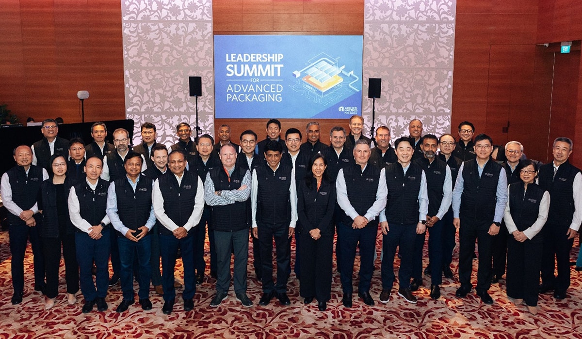
Semiconductor R&D Leaders Share Vision for Accelerating Advanced Packaging
Applied Materials recently convened advanced packaging leaders from across the chipmaking ecosystem to discuss the grand challenges and opportunities to delivering energy-efficient computing for the AI era. A report from the inaugural 2024 Leadership Summit for Advanced Packaging highlights the need for industry-wide, global collaboration to accelerate innovation in foundational semiconductor packaging technologies and address a looming talent shortage.
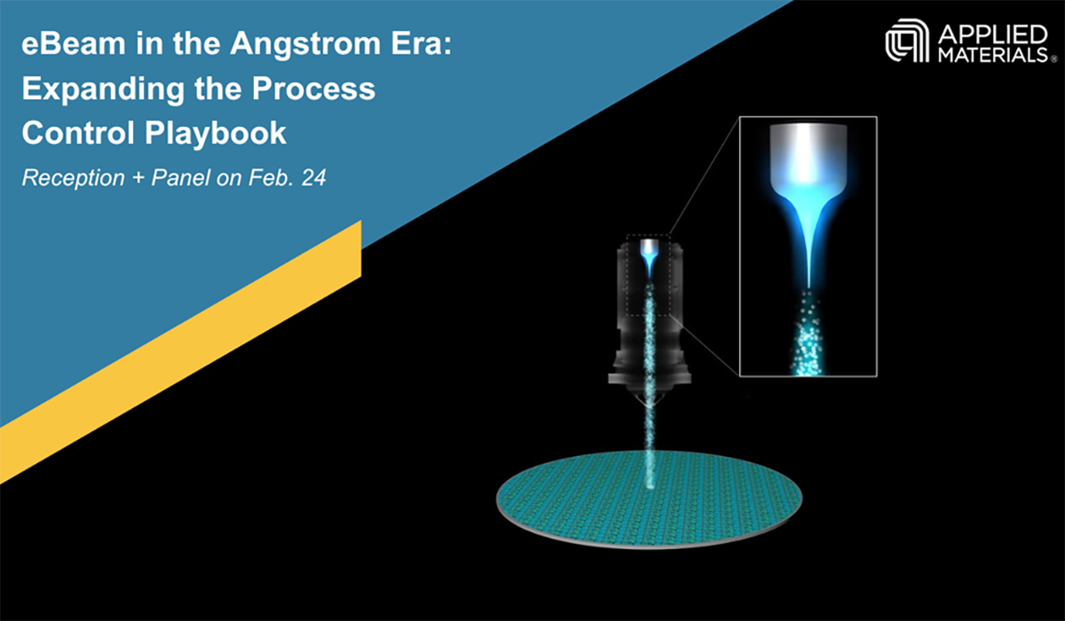
Expert Panel To Explore Advances in eBeam Technology
Alongside the 2025 SPIE Advanced Lithography + Patterning conference in San Jose, CA, Applied Materials will bring together a panel of experts from across the semiconductor ecosystem to explore how chipmakers are increasingly using electron beam (eBeam) technology to continue pushing chip scaling to its limits.

Advanced Packaging Enters a New Dimension
Applied Materials recently hosted a panel during IEDM in San Francisco titled, “The Future of Advanced Packaging: 3D is Here, Now What?” In a lively discussion, technology leaders from AMD, Intel, Cadence and Applied offered their perspectives on a wide range of topics – from the key technology building blocks that will enable next-generation AI chips, to how the ecosystem can work together to accelerate the pace of innovation.

Happy Holidays From Applied Materials
Happy Holidays to all of our readers, and we wish you a wonderful 2025! This year we celebrate our vision to Make Possible® a Better Future. Thanks to connected devices and cutting-edge technology, we're heading into a new era of innovation and togetherness.

Celebrating 30 Years of Display Innovation
While Applied Materials is best known for providing the machines that produce the world’s logic and memory chips, we also have a long history of using our differentiated materials engineering capabilities to solve technology challenges in adjacent end-markets.
Bringing eBeam Review to Compound Semiconductors
The power electronics industry has seen a resurgence in the past two decades – driven first by the advent of specialized power management chips for smartphones and tablets, and more recently by the major global transition to renewable energy sources and electric vehicles. At the heart of this transition lies the power semiconductor device, which modulates the flow of electrical energy to suit the demands of the application.

Implant Innovation Enables the Compound Semiconductor Roadmap
AI may have taken center stage among the drivers for chip industry growth, but there is another global inflection fueling the semiconductor roadmap: the clean energy revolution. Featuring major structural shifts to renewable energy sources, smart grid technologies and electric vehicles, the star player in clean energy is the power semiconductor, which controls and converts electrical energy to supply power for a wide variety of electronic devices.
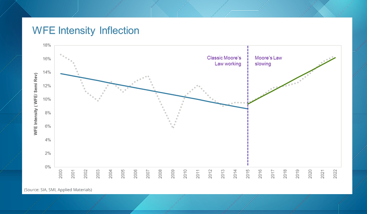
Understanding the Inflection in Wafer Fab Equipment Growth
At Applied Materials, we believe the wafer fab equipment (WFE) market is positioned for strong growth in the coming years, with the potential to grow as fast or faster than the broader semiconductor industry. To better understand the context behind this expectation, my latest blog takes a look back at some of the critical factors that helped bring the WFE sector out of its long period of flat growth in the early part of this century.

Materials Engineering: The True Hero of Energy-Efficient Chip Performance
To better understand the impact of materials engineering on the semiconductors powering our digital world, we analyzed one of the most advanced 3nm chips available today. Our analysis found that less than one quarter of the process steps actually leave a materials footprint on the chip, and yet these materials engineering steps have an outsized impact on performance, power and reliability characteristics.

Applied Materials Employees Rally Together for Environmental Sustainability
During this year’s EarthWorks environmental campaign, more than 2,500 Applied Materials employees mobilized to protect our planet. In this blog, we highlight how our teams around the world made a difference in their communities by inspiring action for environmental sustainability.

The Race for AI Leadership is Fueled by Materials Engineering
At our SEMICON West Technology Breakfast, Applied Materials highlighted how materials engineering innovations are enabling advances in logic, DRAM, high-bandwidth memory and advanced packaging to deliver more energy-efficient AI computing platforms.
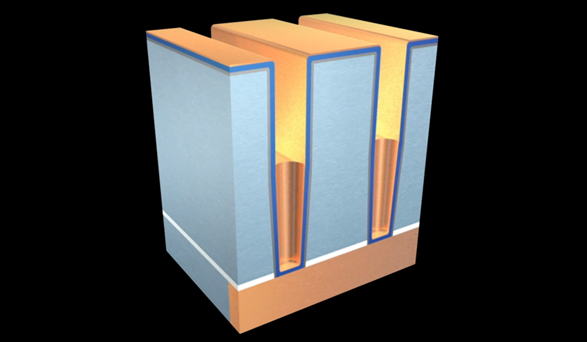
Beyond Backside Power: Scaling Chips to 2nm and Beyond Also Requires Frontside Wiring Innovations
While the industry looks forward to the benefits of backside power architectures, logic scaling depends on wiring innovations on the front side of the wafer as well. At our upcoming SEMICON West Technology Breakfast, Applied Materials will unveil innovations designed to extend the life of copper to 2nm and beyond.
Materials Innovations Can Help Make Quantum Computing a Reality
The Applied Materials Open Innovation Workshop on Quantum Technology brought together global leaders from industry, academia and the venture community to identify and discuss challenges for quantum technology today and into the future. While innovations are needed across the ecosystem, materials engineering can play a critical role in developing the next generation of quantum technologies.
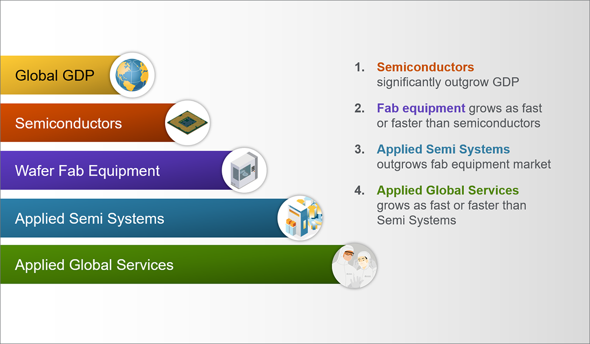
Wafer Fab Equipment Positioned for a New Wave of Growth
The emerging IoT + AI era of computing is expected to double the size of the semiconductor market, bringing it to $1 trillion dollars by the end of the decade. At Applied Materials, we believe the equipment industry can continue to grow as fast or faster than the semiconductor industry on a through-cycle basis. In this blog series, I outline Applied’s framework for the evolution of the fab equipment market.

Power-Hungry AI Applications Demand More Energy-Efficient Computing
While the semiconductor industry has historically driven remarkable improvements in performance-per-watt, the rise of power-hungry AI data centers is pushing the need for energy-efficient computing to an entirely new level.
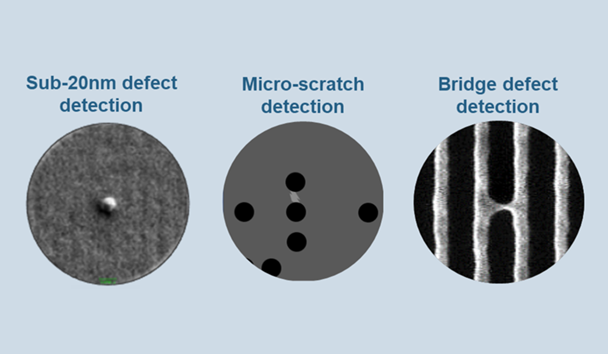
Advanced Logic and Memory Need New Tools for Optical Wafer Inspection
Patterned wafer inspection has always been critical to controlling and perfecting the chipmaking process. However, as chip structures become ever smaller and the process grows in complexity, the way we inspect leading-edge chips needs to evolve. Chipmakers need new capabilities that maintain the high throughput and low cost-of-ownership that is characteristic of “darkfield” inspection, while delivering optimal sensitivity for 3D surface defects and patterned defects.
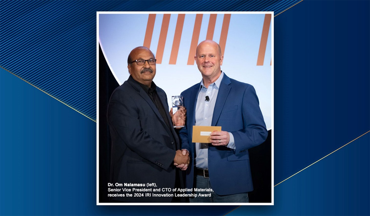
Celebrating Innovation: Dr. Om Nalamasu Receives the 2024 IRI Innovation Leadership Award
A world-renowned expert in materials science, Dr. Om Nalamasu, Senior Vice President and CTO of Applied Materials, was recently recognized by the Innovation Research Interchange (IRI), the National Association of Manufacturers’ innovation management division, with the 2024 IRI Innovation Leadership Award. The award celebrates visionary leaders whose exceptional contributions and transformative influence have significantly advanced the landscape of innovation.
...
Showing 1-21 of 191