Products & Technologies
Products & Services
Company
Contact
Back to Menu
Products & Services
Products & Technologies
Services
Resources
Company
Contact
Solar
Solar
Technology
Specialties
Printed Electronics
Applied PECVD 5.7™
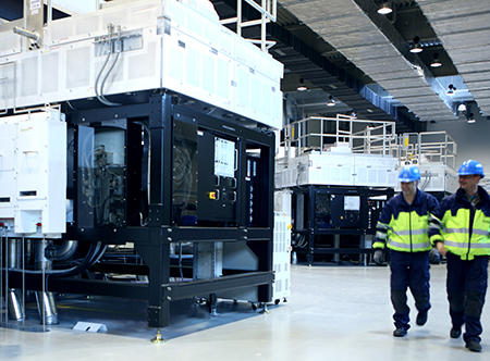
The Applied PECVD 5.7 system deposits the active layers of thin film silicon solar panels on glass substrates up to 5.7m2 in area – the largest in the world. The PECVD 5.7 system is based on Applied’s industry- leading AKT systems for TFT-LCD display manufacturing, proven in over 800 installations worldwide.
The Applied PECVD 5.7 is a single substrate processing system with 7 independent chambers clustered around a central transfer module. It features dedicated amorphous and microcrystalline deposition chambers to eliminate the risk of cross-contamination between the absorber layers of multijunction cell technologies.
- High deposition rate (>500Å/minute for microcrystalline films) enables increased productivity.
- Improved uniformity to enhance cell conversion efficiency.
- Production-proven platform with high uptime (>90%) and superior reliability.