Products & Technologies
Back to Menu
Products & Technologies
Services
Resources

semiconductor and display equipment company


We help put the "silicon" in Silicon Valley and play a vital role in the evolution of the electronics industry.
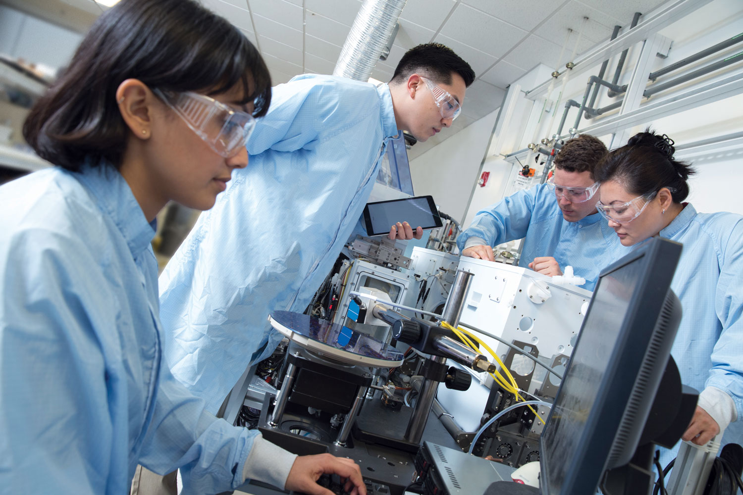
We are the leader in materials engineering solutions used to produce virtually every new chip and advanced display in the world. For more than 55 years, our innovations have improved the lives of billions of people around the globe who may never know us by name, but who rely on us every day as they interact with technology.
The world’s brightest minds—visionaries, engineers, scientists—bring their expertise in materials engineering and come together at Applied with a collection of diverse opinions, experiences and backgrounds to Make Possible better ideas and breakthrough innovations.
Our innovations Make Possible® a Better Future.
This is the Story of an Adventure
It began in 1967 when a group of entrepreneurs joined to create a chemistry supply company called Applied Materials Technology. Over the next 55 years, that small venture transformed into a global leader. The people of Applied Materials, their discoveries, and the products they create provide the foundational building blocks for the semiconductor industry.

Make Possible Starts Here
Our systems make semiconductor devices called chips—the brains of the electronics used in almost every aspect of our lives. The technologies we create are the foundational building blocks of future electronics that Make Possible a Better Future.

Changing How Chips Are Made
Applied is enabling improvements in power, performance, area, cost and time-to-market (PPACt™) of semiconductor devices at a time when the need for semiconductor innovation has never been greater. The breadth of our portfolio, including our Integrated Materials Solutions, allows us to combine technologies in new, innovative ways that unlock the potential of AI and other technology inflections.
Today’s semiconductor customers require faster, more efficient chips to enable increased performance. Applied’s materials engineering expertise includes Integrated Materials Solutions that combine multiple processes with customized metrology and sensors in a single system to help our customers create faster, more efficient chips.
Increasing chip performance to meet the demand of the complex processing required of semiconductors in areas such as AI is realized by lowering power consumption. Applied’s PPACt playbook provides innovative materials engineering solutions to enable higher performance for the AI era.
As the industry moves to smaller process nodes, the amount of space available on a chip to pull transistors closer together is disappearing. Applied’s suite of materials-shaping solutions enable creative ways to scale area and cost while improving power and performance.
Applied’s investments in digital infrastructure bring together sensors, metrology, data science, machine learning and simulation to shorten product development cycles; speed up transfer of new technologies from lab to fab; and optimize cost, output and yield for our customers.
Discovering the Next Breakthrough
Today, in labs around the world, our scientists are developing technologies and using materials in ways no one would have thought possible. We foster an innovation network through venture investments and joint research and development programs with universities, customers, partners and research institutes.
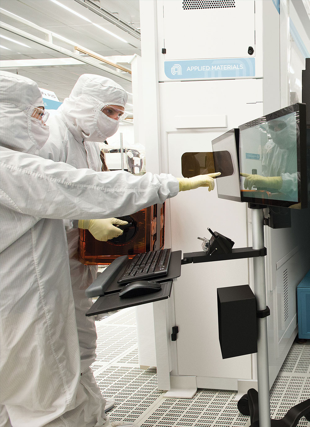
Building Incredible Products
Our worldwide manufacturing operations assemble, integrate and test the various proprietary and commercial parts, components and subassemblies used to build our systems. Our volume manufacturing is centered in Austin, Texas and Singapore, with additional facilities in Germany, Israel, Italy, Korea, Taiwan and the United States.
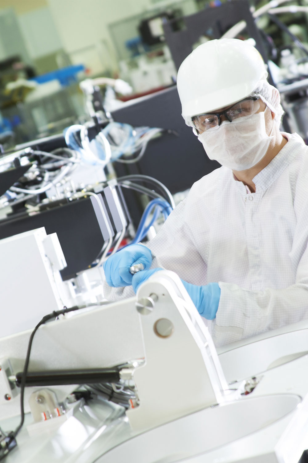
The Heart of Our Organization
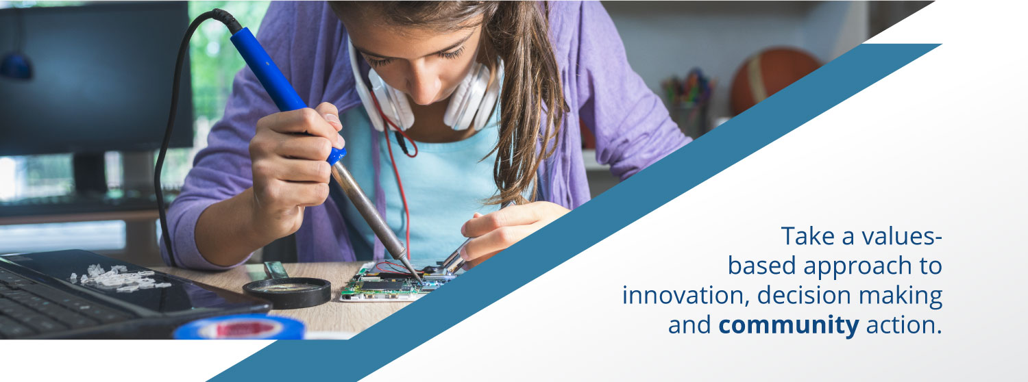
Our values define who we are as a company, inspire us to be better and drive our success.
WINNING TEAM
Achieve great results together in an environment where employees can do their best work
RESPONSIBILITY & INTEGRITY
Operate with mutual trust and respect
MOST VALUED PARTNER
Collaborate broadly to solve our customers’ high-value problems
WORLD CLASS PERFORMANCE
Create a competitive advantage and deliver superior results that generate value and fuel growth

