Products & Technologies
Products & Services
Contact
Products & Services
Products & Technologies
Services
Resources
Contact

Want to be part of enabling today's exciting technologies like AI?
51,000+
installed systems worldwide supported by Applied Global Services

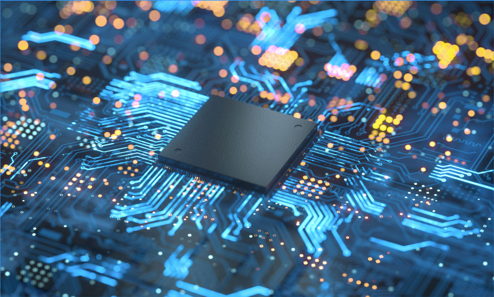
Our materials engineering innovation is at the heart of the electronics you use every day.
Building the foundation of all electronics
Learn about materials engineering and why it's so critical to the future of high-tech innovation.
Keep the Connection going.
Keep up-to-date with news, announcements and jobs by following us on LinkedIn.
We’re Changing the Rules to Accelerate Innovation
In 2023, Applied Materials announced the Equipment and Process Innovation and Commercialization (EPIC) Center in Silicon Valley representing the largest-ever U.S. investment in advanced semiconductor equipment R&D. It is designed from the ground up to dramatically reduce the time it takes to commercialize breakthrough technologies from early-stage research to full-scale manufacturing. It does this by increasing speed, accuracy and efficiency through tighter collaboration and faster cycles of learning.
With state of the art cleanroom space for collaborative R&D, the EPIC Center is on track to become operational in 2026.

Science + Innovation = Materials Engineering
Materials engineering uses the properties and structures of materials to drive innovation. Our tools create semiconductor chips—the brains of your phone, game console, smart watch, VR headset and so much more.

Material Innovation and Physical AI
Ever increasing demand for AI is driving the need for high-performance, energy efficient computing. AI is reshaping the semiconductor roadmap and changing the way chips are designed and manufactured.
Physical AI refers to AI systems in machines that can sense, reason, decide, act and learn in the physical world. These can be humanoid robots, autonomous vehicles or other devices like cameras or other wearables.
In particular, physical AI and humanoid robots represent a transformative wave in robotics, merging digital intelligence with physical action. Humanoid robots push the semiconductor industry forward by requiring new innovation in chip architectures, new materials and power devices that are capable of continuous operation. For Applied Materials, this transformation is directly tied to the accelerating demand for advanced semiconductor materials technologies that enable autonomy, sensing, and real-time intelligence.
Humanoid robots, as part of the physical AI phenomenon, are a reflection of the convergence of AI, advanced materials in one efficient system. They require high-performance compute, power electronics like GaN and SiC, and memory solutions. Each of these components is built on materials technologies that Applied Materials develops and scales. Our advanced materials engineering is foundational to enabling physical AI.
Physical AI will only reach its full potential if the power and compute infrastructure behind it continues to advance—this is a challenge the Applied is uniquely positioned to solve.
#MakeItMaterial


- 1 / 4
- 2 / 4
- 3 / 4
- 4 / 4
Get to Know Us