New Metrology and Inspection Technologies Needed for More-than-Moore Markets
By Daniel Harel and Mike Rosa, Ph.D.
The escalating costs of following Moore’s Law have shifted the semiconductor industry’s focus to More-than-Moore (MtM) technologies, where analog/mixed-signal, RF, MEMS, image sensing, power or other technologies may be integrated with CMOS in a variety of planar, 2.5D and 3D architectures.
The integration of these and other key technologies is enabling a host of fast-growing applications like artificial intelligence, IoT infrastructure products and automotive radar, to name just a few.
Earlier this year, Yole Developpement estimated the growth of the MtM market as approximately 74M wafers (of all sizes) annually through 2023, with a compound annual growth rate (CAGR) of ~3%. 1 But looking only at the most popular wafer sizes (12”, 8” and 6” wafers), the projection becomes 60M wafers by 2023, for a CAGR of about 5%. Six-inch wafers remain a significant portion of the market because new technologies in silicon carbide (SiC) power and gallium arsenide (GaAs) photonics-based applications continue to grow even as overall demand for six-inch wafers declines at a rate of about 5% per year, as applications continue their migration to 8” wafers.
The fact that MtM markets have become significant sources of semiconductor demand is good news for semiconductor manufacturers. But it means that new metrology, inspection and defect review approaches are needed to accommodate the wide variety of possible failure modes that may impact these multi-technology devices.
For example, consider consumer and automotive applications. Combined, these are most definitely the largest unit volume users of integrated circuits, but their defect requirements are vastly different and, therefore, each also has different inspection requirements (table 1).
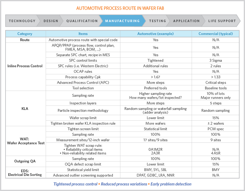
Table 1. Significant inspection differences exist between automotive and commercial application. (Source: Audi AG)
Apple’s iPhone X consists of about 125 integrated circuits (ICs), of which ~19 are produced on 300mm wafers, ~87 on 200mm wafers and ~15 on 150mm wafers (figure 1). It is true that many advanced 300mm applications can make use of traditional node-scaling inspection techniques, but that is not necessarily so for many devices fabricated on 200mm and smaller wafers. These may involve specialty materials and/or may require non-traditional fabrication steps such as wafer bonding, deep reactive ion etch (DRIE), etc.
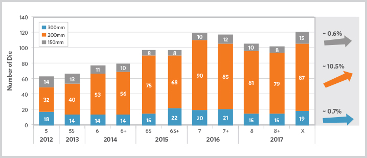
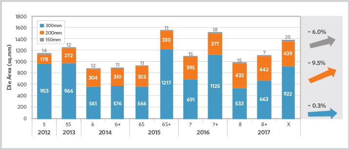
Figure 1. An analysis of iPhone bills of materials (BOM) shows die content by wafer size for iPhones manufactured from 2012 through 2017 (top), and the sum total of IC die by wafer size (bottom). The majority of die area is accounted for by 300mm wafers, but by far the fastest-growing segments are die from 200mm and 150mm wafers. These wafers support most MtM device applications today, including new applications in power and photonics just now making their way into the market. (Source: Applied Materials)
Additionally, given the ongoing and fast-paced introduction of new capabilities and models in consumer electronics products, and the lack of ongoing investment in some of them, the expected product lifetime of most high-volume consumer products like smartphones is typically just a few years. That is why smartphone manufacturers may not hold component suppliers to the same stringent quality and reliability standards prevalent in other industry segments.
Device defect specifications for consumer electronics may be in the range of one part per million (ppm). Assuming typical smartphone manufacturing volumes of 1.5-1.6B units, and using the iPhone BOM mentioned earlier as a figure of merit, one could assume there are roughly 187K or more unsaleable units per year, a conservative number that represents roughly $93M per year of lost product sales.2
Different Industries, Different Standards
Contrast that with the automotive industry (figure 2), where the numbers can add up more rapidly. Cars must operate reliably for many years over widely varying environmental conditions. Thus, there is much less tolerance for “killer” defects, which are now specified in the parts per billion (ppb) range, an order of magnitude higher than for consumer electronics.

Figure 2. ICs are used extensively in today’s cars and their use is growing, making it imperative to find better, faster ways to identify “killer” device defects.
The dollar amount of lost automotive revenue attributable to those defects is also orders of magnitude higher. In addition, the potential impact of failures is qualitatively different as well. Since serious injury or even death can result from failure of automotive components (figure 3), it isn’t entirely surprising that component makers serving the automotive segment have begun speaking in terms of parts per trillion (ppt).

Figure 3. Common defects for Moore-than-Moore (MtM) chips in automotive and consumer applications.
One major semiconductor supplier to the automotive industry, NXP Semiconductor, explained: “The cost of the impact of defect-related failures increases from tens of dollars at the IC level, to hundreds of dollars at the module level, to thousands of dollars at the level of the car.” (table 2).3

Table 2. The value of product sitting idle due to defect-related failures can be substantial in the automotive segment. (Source: NXP Semiconductor)
With passengers' safety at serious risk, chipmakers need to ensure delivery to automakers of virtually zero-defect devices. Therefore, advanced, high-productivity metrology and inspection technologies are essential.
Existing Metrology/Inspection/Defect Review Technologies
Applied Materials offers several metrology, inspection and defect review technologies to identify killer defects in MtM devices before they find their way into finished products (figure 4).
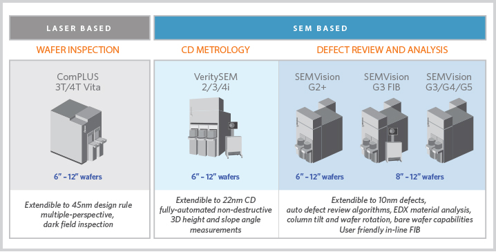
Figure 4. Metrology, inspection and defect review technologies from Applied Materials.
Sophisticated wafer-inspection tools like Applied’s ComPLUS™ 3/4T VITA enable users to detect surface particles, pattern flaws, and other conditions that may compromise a completed device.
Applied’s high-quality, state-of-the-art review tools such as the SEMVision™ G2+/G3 or SEMVision G3 focused ion beam (FIB) use high-resolution imaging and energy dispersive x-ray (EDX) material analysis information for root cause analysis, thereby reducing the cycle times needed to identify failures and drive corrective actions.
Metrology CD-SEM tools such as Applied’s VeritySEM™2/3/4i are used to monitor and control process quality in both lithography and etch steps. Their advanced capabilities for slope and edge analysis provide extensive data that leads to better process-quality assessments and monitoring.
Although these tools represent the current state-of-the-art, development of new and innovative metrology, inspection and defect review techniques are ongoing to meet the unique challenges of MtM devices.
One major issue is that complex architectures which require many layers of processing to create the device stack—whether they are MtM devices or advanced CMOS ICs—impose additional process control challenges. Thus, the ability to find any buried defects which could lead to device failure is of paramount importance.
Indeed, the ability to inspect buried defects, or even to remove layers of material to uncover them, is fast becoming one of the industry’s highest-value problems. Although various tools and technologies exist to examine multi-layer structures, these inspection techniques often result in destruction of the IC or wafer under examination. They are also almost always performed on a wafer or IC that has been removed from work-in-process (WIP) and then analyzed off the production line, leading to production inefficiencies, delays or stoppages, and increased costs.
Thus, a technology that would enable users to perform a fast, accurate multi-layered buried defect analysis in situ—without having to destroy or remove a wafer from WIP—would be invaluable.
For more information, contact daniel_harel@amat.com
[1] “Wafer Starts for More-than-Moore – Market Trends,” Yole Developpement, April 2018.
[2] Assume 125 devices per iPhone. Assuming each IC has a 1 ppm failure rate, then approx. 125 failures per 1500 phones. At roughly $500 per phone, that comes to over $93M.
[3] ‘NXP Total Quality’, April 2018.
