
OLEDS: DISPLAY'S NEXT BIG THING
By Kerry Cunningham
After years of hope and promise, the adoption of large-area OLED displays for televisions, laptops and computer monitors is finally beginning to happen. Larger OLED displays in both traditional and novel form factors are now emerging as an affordable option to traditional LCD technology, thanks to next-generation manufacturing that has dramatically reduced production costs.
New materials engineering strategies, backplanes and fabrication methods have led to higher yields for larger panels, giving rise to thinner, lighter, curved, flexible, foldable and rollable organic light-emitting diode (OLED) displays at increasingly attractive consumer price points. These new displays offer the high picture quality consumers desire and the high performance needed for gaming and virtual reality applications (i.e., a refresh rate of at least 240 Hz).
A key advantage of OLED thin-film transistor (TFT) technology versus liquid crystal displays (LCDs) is that OLED TFT pixels are self-illuminating, while LCD pixels must be illuminated by light-emitting diodes in a backlight unit (BLU) placed behind them. The simpler OLED architecture leads to thinner and more flexible panels with better color range and viewing angles, less motion blur, brighter pixels, higher contrast ratios, cooler running temperatures, and lower energy consumption (Figure 1).
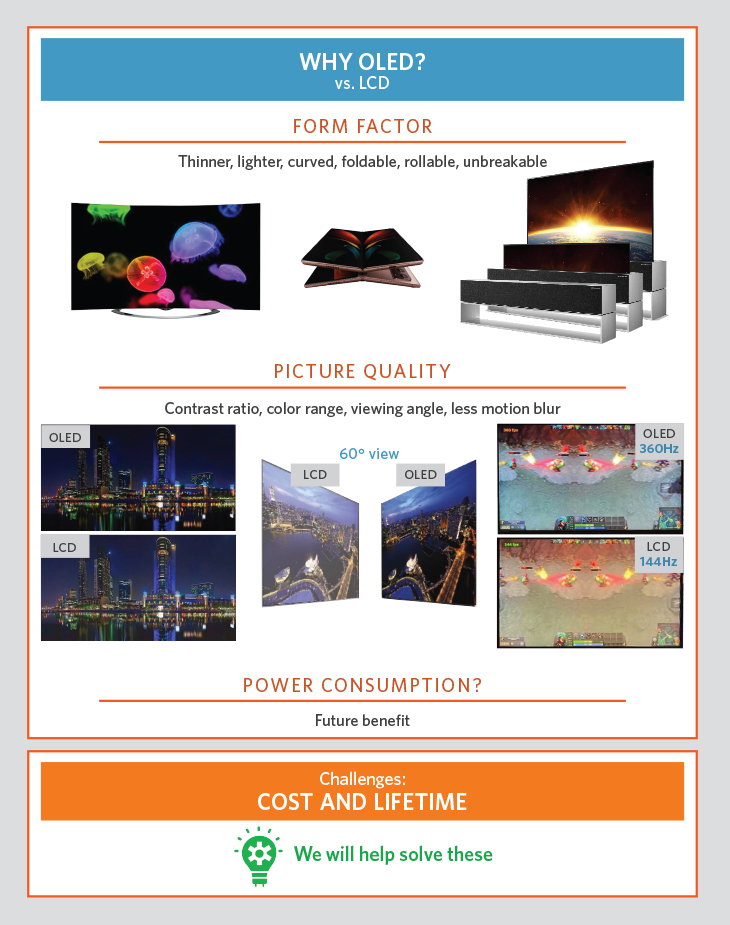
Figure 1. OLED technology makes flexible, foldable and rollable displays possible, with higher image quality. (Source: Applied Materials)
OLED YIELD AND COST CONSIDERATIONS
While these attributes have made small OLED displays the go-to technology for advanced smartphones, LCD technology has long enjoyed one major advantage when it comes to larger-sized panels: much lower manufacturing costs.
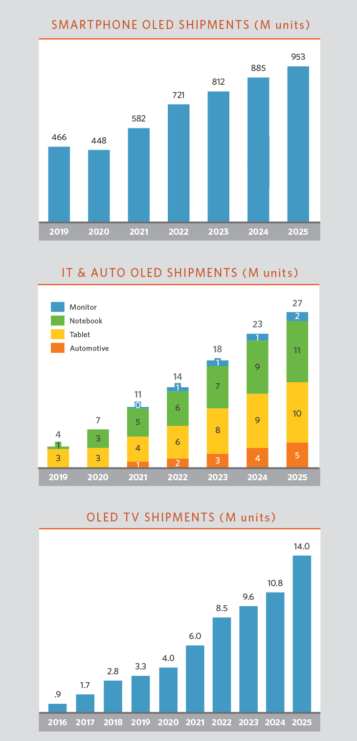
Figure 2. The graphs show the projected use of OLED-based displays in smartphones, IT and automotive products, and television sets over the next decade. (Source: DSCC Quarterly OLED Shipment Report Q3 2020)
The cost differential comes about because although OLED architectures are simpler, the materials engineering and fabrication techniques required to produce them are more difficult. Smartphone price points provide enough margin for manufacturers to use OLED displays, but the technology has enjoyed less success to date in larger displays. However, forecasts (Figure 2) are beginning to show that the future will be brighter for OLED technology in larger-sized applications.
Resolution at 8K is expected to be a major driver of TV demand in the future. But the benefits of 8K go beyond just higher resolution. It provides other features such as a “capture and display” capability that enables users to reframe (i.e., highlight) a region of interest within an overall picture or pan and scan a widescreen image, both at 2K or 4k resolutions. It also allows video frame grabs for still images.
Although 8K works with both OLED and LCD technology, because cost is a major driver of consumer buying habits, consumers will only choose an OLED display over an LCD display if pricing is similar at the same size. Achieving this price parity has been challenging until now: as the portion of substrate glass devoted to one TV screen becomes larger, just one “killer defect” can render a large section of that expensive substrate useless (Figure 3). Thus, higher yields are a critical and high-value challenge for panel manufacturers.
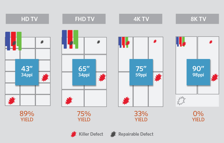
Figure 3. Tighter process control and significant particle reductions to reduce the number of “killer defects” are essential to achieve 8K resolution as the size of TV screens increases. (Source: Applied Materials)
Also, because an 8K Gen10+ TV screen has more than 33 million pixels, reducing the amount of power needed to drive pixel brightness at this resolution is paramount. In each “unit cell” of a flat panel display (FPD), the TFTs, storage capacitor electrodes, signal bus lines and black matrix material constitute opaque areas. The open area through which light can pass is called the aperture.
Accordingly, an important design consideration is to maximize the aperture ratio, letting as much light as possible pass through each unit cell so that less power must be dedicated to display brightness. This requires much tighter process specifications than for previous generations of TV screens, such as ultra-high definition (UHD) (Figure 4).
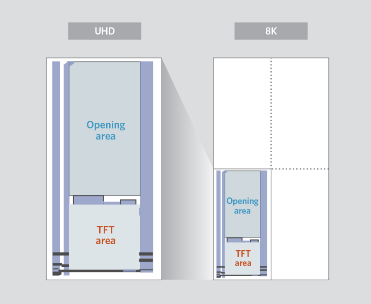
Figure 4. For FPDs at 8K resolution, it is critical to increase the pixel aperture ratio, or the size of the aperture (the open area through which light can pass) versus pixel TFT area. The figure shows the requirement schematically. (Source: Applied Materials)
MOx BACKPLANES
One way to significantly lower the cost of larger OLED displays is to adopt metal oxide (MOx) technology for their backplanes. Compared to traditional low-temperature poly silicon (LTPS) technology, significantly fewer process steps are required to make MOx-based TFTs. This can potentially reduce costs while still achieving electron mobilities that are high enough to meet the required specifications for picture quality performance and refresh rates.
A MOx material called indium gallium zinc oxide (IGZO) enables backplanes with higher aperture ratios, low leakage currents, a high on/off ratio for low power consumption, and device performance stability. These backplanes are emerging as the most effective solution for large-area 8K OLED TVs (Figure 5).
APPLIED’S INTEGRATED MATERIALS SOLUTIONS
Scaling of TFTs is a key consideration for the successful use of MOx backplanes at larger panel sizes, and plasma-enhanced chemical vapor deposition (PECVD) processing is a key enabler for cost-effective scaling (Figure 6). The most important scaling requirement is the ability to achieve a high degree of film uniformity for both SiO and SiN films, which can best be achieved by single-chamber processing. A high degree of temperature control and uniformity, plus plasma confinement for high-power processing, are also essential to producing high-quality TFTs for use at larger sizes.
However, IGZO poses a significant fabrication challenge because it tends to interact with its surroundings during device fabrication. Its properties can change as a result, affecting device performance. That means great care must be taken during all of the device fabrication/integration process steps: CVD, PVD, dry etch and annealing.
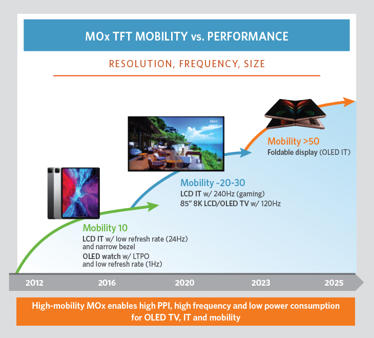
Figure 5. This figure shows the relationship between MOx TFT mobility vs. performance in different display sizes. (Source: Applied Materials)
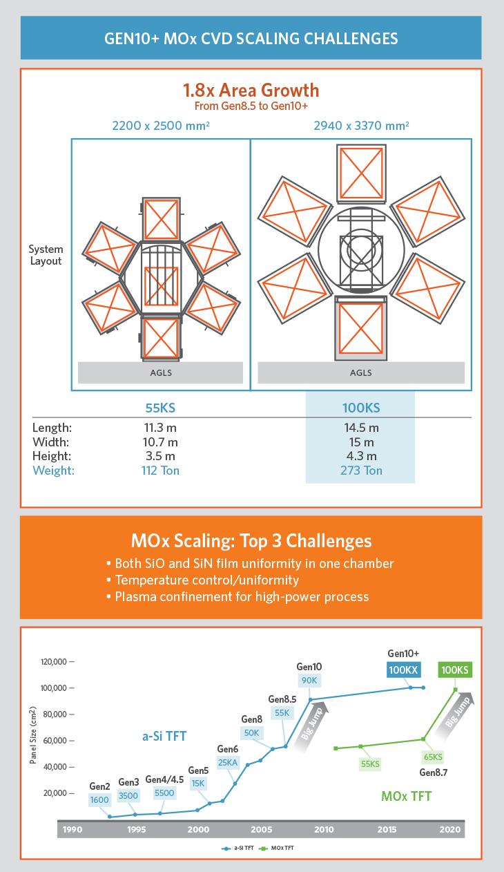
Figure 6. PECVD processing enables the cost-effective scaling of MOx backplanes. The figure shows the history of the use of PECVD at different panel sizes. (Source: Applied Materials)
Oxygen and hydrogen balancing is important in the fabrication of IGZO films. The key to producing uniform and stable IGZO TFT devices is to tightly control the oxygen levels/vacancies and hydrogen levels during each fabrication step (Figure 7). Tight control leads to improved insulators for the top-gate (TG) TFTs used in OLED technology, while high-quality SiOx deposition reduces interface trapping and minimizes hydrogen content in the CVD layer, leading to reliable device performance.
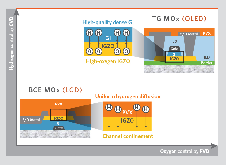
Figure 7. Device integration of top-gate (TG) MOx improves MOx device performance. (Source: Applied Materials)
In addition, the use of a self-aligned TG architecture for MOx TFTs, versus a more traditional bottom-gate approach, has a key advantage for OLED displays: It enables shorter TFT channel lengths, making it easier to design physically larger, higher-resolution screens and to increase the drive frequency (Figure 8).
The Applied Materials Display Flexible Technology group offers a single-chamber, integrated materials solution that couples Applied’s proven CVD and PVD technologies for production of MOx films with best-known methods (BKMs) to integrate both of those technologies in one uniform film, even though they have different film properties.
This enables users to achieve the device performance required in hydrogen diffusion control for high-quality dense gate insulators, and the oxygen control and oxygen vacancy levels required to fabricate high-quality IGZO films.
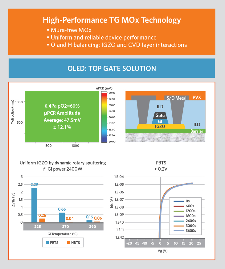
Figure 8. An optimum oxygen/hydrogen balance in IGZO and CVD layer interactions improves top-gate (TG) MOx device performance. (Source: Applied Materials)
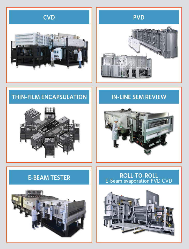
Figure 9. As the world’s leading supplier of display equipment in 2019, Applied Materials’ display and flexible manufacturing tools are key enablers in the G10+ TV and mobile OLED segments. (Source: DSCC)
A VIEW OF THE FUTURE
OLED displays deliver image quality that is superior to other technologies, and although they are more difficult to manufacture, new tools exist to simplify fabrication. Manufacturing tool suites up to Gen 10+, such as those from Applied Materials (Figure 9), are helping suppliers drive down costs, enabling them to offer computer displays and TVs with significantly higher image quality at more affordable price points. In 2019, for example, 8K televisions hit the market at prices ≥$3,500, but prices have been coming down since then.
The OLED revolution has started!

Kerry Cunningham is Display Flexible Technology Product Marketing Manager for Applied Materials. For additional information, contact him at kerry_cunningham@amat.com