Products & Technologies
Products & Services
Contact
Back to Menu
Products & Services
Products & Technologies
Services
Resources
Contact
Posted
April 29, 2025
eBeam Breakthrough Finds Defects Hidden Deep Inside Chips
A new feature article in IEEE Spectrum magazine examines the technology breakthroughs behind Applied Materials’ new SEMVision™ H20 defect review system.
Why It Matters: In the angstrom era of chipmaking, even the smallest defect can compromise chip performance and the yield of the manufacturing process. Distinguishing true defects from false alarms, or “nuisance defects,” has become increasingly difficult. Traditional defect review systems are struggling to keep pace with the demands of modern chip manufacturing. The industry is at an inflection point, where the ability to detect, classify, and analyze defects quickly and accurately is no longer just a competitive advantage – it’s a necessity.
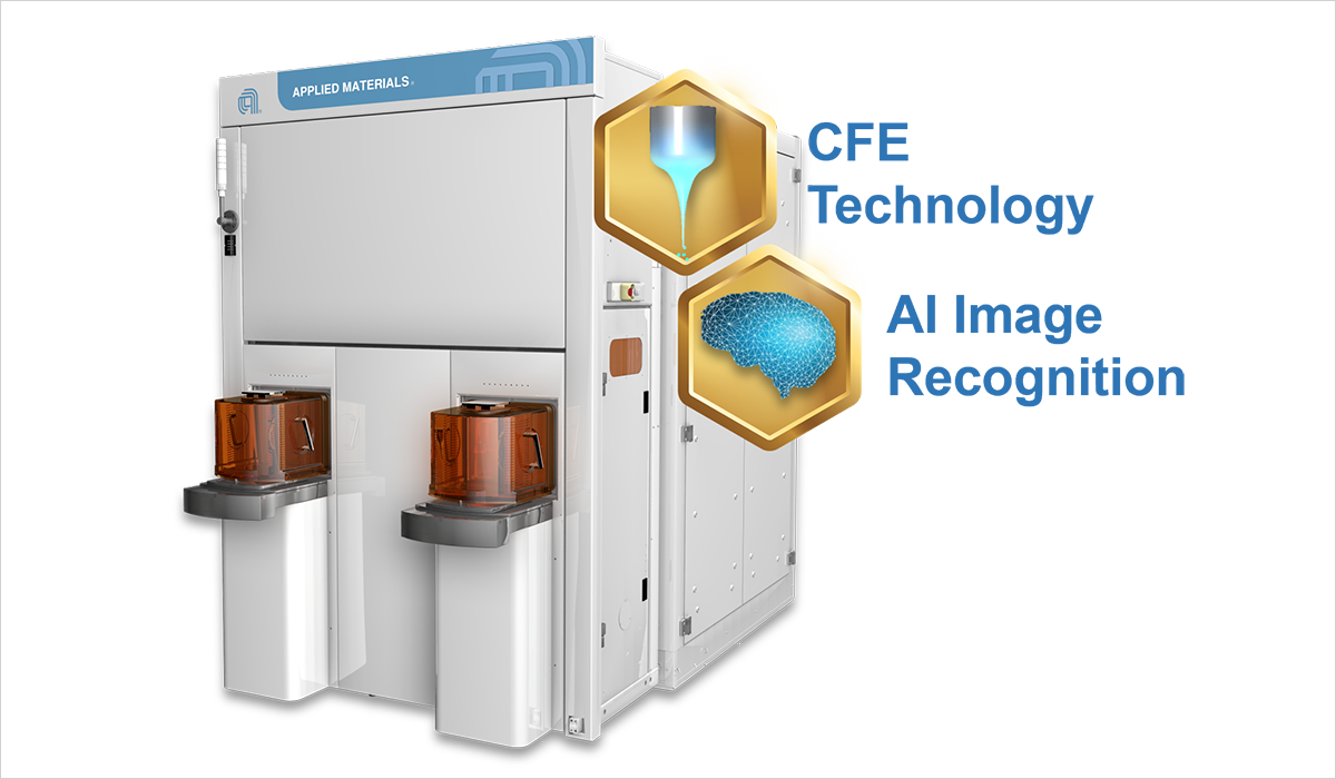
Behind the Breakthrough: In response to these challenges, Applied developed the SEMVision H20 system, a faster and more accurate defect review system that can analyze exponentially more samples without sacrificing sensitivity or resolution. A critical enabler of this innovation is cold field emission (CFE) technology, a breakthrough that has redefined the capabilities of electron beam (eBeam) systems. Operating at room temperature, CFE produces a narrower, more stable beam with a higher density of electrons that results in significantly improved resolution and imaging speed compared to traditional thermal field emission (TFE) technology. For decades, CFE systems were limited to lab usage because it was not possible to keep the tools up and running for adequate periods of time. After more than 10 years of research, Applied engineers solved the reliability issues and in 2022 introduced the industry’s first eBeam systems based on CFE technology.
Adopting AI: While CFE technology provides the foundation for high-resolution defect detection, the sheer volume of data generated by modern inspection tools has created a new challenge: how to process and analyze this data quickly and accurately. The SEMVision H20 system uses AI algorithms to sift through massive datasets, identifying patterns and anomalies that would be impossible for human engineers to detect manually.
“One of the biggest challenges chipmakers often have with adopting AI-based solutions is trusting the model,” said Neta Shomrat, who leads marketing for the SEMVision product line. “The success of the SEMVision H20 validates the quality of the data and insights we are bringing to customers. The pillars of technology that comprise the product are what builds customer trust. It’s not just the buzzword of AI. The SEMVision H20 is a compelling solution that brings value to customers.”

Neta Shomrat, SEMVision Product Marketing, Applied Materials
Dig Deeper: To learn more about the innovations enabling Applied’s newest eBeam system, read the article in IEEE Spectrum, the flagship publication of the Institute of Electrical and Electronics Engineers.