Products & Technologies
Products & Services
Contact
Back to Menu
Products & Services
Products & Technologies
Services
Resources
Contact
Posted
April 04, 2025

Stay updated on our content.
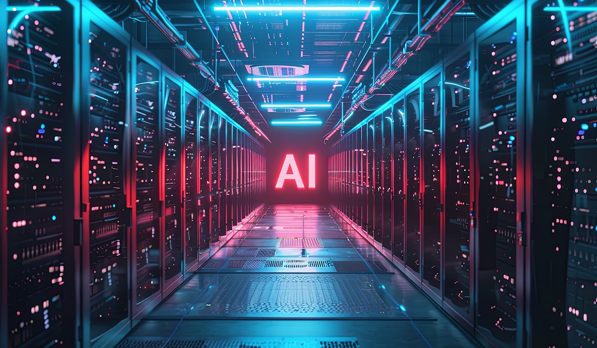
Optical Circuit Switches Show Promise for More Energy-Efficient AI Data Centers
by Steven Konsek and Walter Liu
In today’s rapidly evolving tech landscape, the demand for massive power and higher speeds to transport data between GPUs for training ever-expanding large language models presents a significant challenge for cloud computing service providers. While electrical packet switches (EPS) are approaching their technical limits, optical circuit switches (OCS) offer a promising solution.
Unlike traditional EPS – or even EPS with co-packaged optics – OCS uses all-optical connections to link GPUs via switched ports and optical transceivers. This architecture enables significantly higher bandwidth over kilometer distances while consuming much less power. In AI clusters, OCS can form an all-optical network, improving efficiency and scalability.
Applied Ventures co-led the Series A funding for startup Salience Labs because of its innovative OCS based on Semiconductor Operational Amplifier (SOA) technology, which delivers exceptionally low latency and insertion loss. Salience Labs offers its SOA-based OCS Photonic Integrated Circuit in two configurations: a higher radix switch for high-performance computing and a lower radix version to minimize impact radius for AI data centers. This flexibility allows Salience Labs to tailor its solutions to different performance and cost requirements for a variety of customers, from hyperscalers and GPU vendors to high-speed traders at financial institutions.
Beyond addressing the technical challenges of building high-speed, long-reach networks, the semiconductor industry must also focus on reducing the carbon footprint and tackling the unsustainable power consumption of AI data centers. According to the Energy Information Administration, U.S. data centers will consume 6.6 percent of the country’s total electricity by 2028, more than double the 3 percent recorded in 2024[1]. Total power consumption in AI data centers includes electricity used by computing elements such as GPUs and networking gear such as switches and transceivers.
To slow the rapid growth of energy consumption, both established companies and startups are innovating in chip design and new system architecture. For example:
- Google’s TPU design goal is to deliver 10 times the total cost of ownership efficiency compared to GPUs by using customized accelerators for specific AI workloads[2].
- Lumentum estimates the power used in networking data between GPUs and memories per training run will increase from 21.5MW for GPT-4 to 122MW for GPT-5[3]. Using energy-efficient optical (EEO) interfaces and OCS can reduce total networking power during GPT-5 training by 79 percent, which is similar to GPT-4.
- Arista Networks estimates that EEO interfaces, which include co-packaged optics and linear-drive pluggable optics, can save up to 20W per module at 1,600Gbps[4].
OCS has the potential to replace EPS to meet the high-bandwidth, long-reach requirements to scale-up and scale-out tens and hundreds of GPUs, while allowing these computing elements to act as one supercomputer.
Applied Ventures is actively investing in photonics startups to foster a vibrant ecosystem to build high-speed, energy-efficient networks for next-generation data centers. Combining these investments with internal R&D, Applied Materials is enabling scalable AI computing and supporting a sustainable future with technology innovation.
___________________________________________
[1] 2024 United States Data Center Energy Usage Report. Lawrence Berkeley National Laboratory, Berkeley, California.
[2] Cliff Young, TPU Architect from Google Deepmind, “Codesign from Semiconductors to AI” presentation at CASPA Annual Conference 10/7/2023
[3] Lumentum white paper “Energy Efficient AI Networks Lead to Dramatic Reduction in Environmental Impact ”
[4] Andy Bechtolsheim from Arista Network, Sustainable Optics for Scaling AI, OCP 2024
Steven Konsek
Investment Director, Applied Ventures

Steven Konsek is an Investment Director at Applied Ventures where he focuses on photonics and displays in addition to supporting investments and startup ecosystem engagement in Europe and Israel. Prior to joining Applied Ventures in 2022, Steven spent nearly two decades working with and funding deep-tech startups in the U.S. and Europe. He was most recently Director of Business Development at Aledia, a French photonics startup. Prior to Aledia, Steven led innovation programs at the U.S. National Science Foundation, where he ran NSF’s portfolio funding startups in the semiconductor, photonics, advanced materials and IoT sectors as well as leading the Innovation Corps program for deep-tech startups. Prior to NSF, Steven held leadership positions in several semiconductor/photonics startups, including Illumitex, Glo/Qunano and Nantero. Steven has a Ph.D. in physics from the University of Washington and BS in mathematics from Purdue University.
Walter Liu
Principal, Applied Ventures

Walter Liu is a Principal at Applied Ventures. As a passionate investor and value creator for his entire career, Walter has led both strategic and financial venture investments for multi-international technology corporations since 2016. His venture capital investments have spanned across AI, semiconductors, cloud, mobile, automotive, IoT and enterprise software. Before joining Applied Ventures, Walter was the Head of US investment at MediaTek Capital. Prior to transitioning into venture capital, Walter was a senior strategic marketing manager at Qualcomm and a wireless product manager at Huawei and Nokia. He also has seven years of ASIC application and system engineering experience at Qualcomm, Motorola and LCC International, where he designed AT&T’s CDMA network in Los Angeles and supported base station OEMs to deploy 3G networks around the world. Walter has an MBA in finance and entrepreneurship from Cornell University and an M.S. in electrical engineering from UCLA.