Products & Technologies
Products & Services
Contact
Back to Menu
Products & Services
Products & Technologies
Services
Resources
Contact
Posted
April 17, 2025

Stay updated on our content.
The Chip Industry Needs Sustainable Tech Startups

by John Wei and Blair Georgakas
The resource demands of high-performance computing for the AI era are reinforcing the semiconductor industry’s need to act as environmental stewards. According to the Energy Information Administration, U.S. data centers are projected to consume 6.6% of the country's total electricity by 2028, which is more than double the 3% recorded in 2024[1]. The very manufacturing infrastructure that enables these breakthrough technologies and improves the lives of millions is itself consuming more energy, water and materials while generating emissions through industrial processes and rising electricity use. These environmental factors have motivated the chip sector’s largest manufacturers to establish long-term sustainability goals and invest heavily in technology innovations to meet these challenges.
Startups for Sustainable Semiconductors
Recognizing that these sustainability goals could not be achieved through incremental improvements alone, a group of corporate venture investors from the top-tier semiconductor companies devised a grassroots initiative: the Startups for Sustainable Semiconductors (S3) pitch event in collaboration with SEMI. The mission of S3 is to bring sustainability-related innovations to semiconductor operations through mentoring, pitch-development and customer access.
Since its inception in 2021, S3 has vetted more than 150 unique startup teams, leading to eight direct VC investments and 34 first-of-their-kind proofs of concept. Seven of the participating startups successfully scaled their technology into initial production at semiconductor manufacturing sites in areas such as water, energy usage and emissions mitigation.
Breaking the Barrier to Entry for Sustainable Startups
For advanced semiconductor manufacturing, there is no “one-size-fits-all” approach. This creates a relatively high barrier to entry for startups seeking to help chipmakers curb the environmental effects of industrial manufacturing.
The sheer complexity of chip production is daunting – a single device requires more than 300 individual process steps. Only a handful of the largest companies have the ability to produce these complex chips at high volume. This global consolidation has created technology islands of IP and design know-how where one company’s challenges require bespoke solutions that are not easily addressed by outside innovators. And because semiconductor manufacturing is highly proprietary, it requires a degree of data privacy and security that typically precludes chipmakers from openly discussing their production processes.
A vital component of the S3 program is the mentoring sessions offered to the semifinalists with the intention of helping startups break into the semiconductor industry. Corporate investors and technology experts are paired with startups to provide guidance on semiconductor-specific technical challenges, whether they’re focused on water reclamation, emission abatement or PFAS destruction technologies.
Finding the Right Technology Innovations
Each year, three categories are chosen to reflect the most up-to-date thinking of where and how the semiconductor industry needs to tackle sustainability. While water, energy, and materials have consistently been areas of focus, now in its fourth year, the original semiconductor manufacturing topics propagated by S3 have expanded to include GenAI and datacenter sustainability, reflecting downstream pressures to reduce energy footprint for AI-powered solutions with topics:
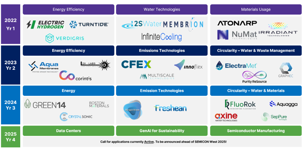
Figure 1: Startup Finalists by Category, since S3 program inception
Measuring and Rewarding Successful Startups
The mission of the S3 program is to identify startups that can:
- Deliver real-world value to semiconductor use cases
- Scale in a timeframe that aligns with the decarbonization goals of our companies
- Provide opportunity for venture-style return on investment
S3’s success metrics showcase examples of how applicants and their solutions have been assessed, contacted and invested. Data collected since 2021 shows:
- 1 in 3 applicants moved into the proof of concept (POC) stage.
- 1 in 5 that secured a POC moved into a scaled deployment.
- 1 in 2 in scaled deployment received direct investment from a member VC arm.
- About 1 in 30 completed a successful first scaled deployment with a chip customer.
As one 2024 S3 finalist said, “The S3 competition hits the mark for any startup engaged with the semiconductor manufacturing industry. Such a focused event was exactly what helped give us the boost of exposure we needed to advance our startup journey.”
A Call to Action
The industry’s sustainability journey is not only a response to pressing environmental concerns, it’s a strategic adaptation to evolving regulatory landscapes and shifting consumer expectations. We encourage interested parties to heed our call to action. There are three, one for each target audience:
- To startups – we want to hear from you! Please apply or reach out to our member companies to learn more.
- To stakeholders across the semiconductor industry – we want to work with you! S3 is volunteer based and carries no cost commitment to participating corporates.
- To other industries pursuing similar decarbonization efforts – we want to learn with you!
S3 is a work in progress and an important step in bringing sustainability to the semiconductor sector. The positive momentum and early metrics are encouraging, yet the challenge of infusing sustainability innovations into the rapidly evolving semiconductor industry and making a tangible impact remains a daunting task. We look forward to your ideas, insights, and active participations as we continue this important work.
[1] 2024 United States Data Center Energy Usage Report. Lawrence Berkeley National Laboratory, Berkeley, California.
John Wei, Ph.D.
Senior Investment Director, Applied Ventures

John Wei is a senior investment director at Applied Ventures, where he specializes in venture investments in semiconductors, computing infrastructure, AI/ML, advanced manufacturing, advanced materials and sustainability. Prior to joining Applied Ventures, John was a key member of the SABIC Ventures investment team, where he led multiple investments in advanced materials, display, energy & sustainability, and manufacturing in North America, Europe, and China. John has a bachelor’s degree from Tsinghua University and a Ph.D. from Rutgers University, both in chemical engineering. While at Rutgers, he also earned a master's degree in computer science. In addition, John holds an M.B.A from UCLA with a focus in finance and entrepreneurship.
Blair Georgakas
Investment Manager, Applied Ventures

Blair Georgakas is an investment manager at Applied Ventures. She has a broad set of interests across deep tech / hardtech verticals and is currently supporting investments in energy storage and additive manufacturing. Prior to joining Applied Ventures, Blair led the physical product management team for 3D printing start-up, Shapeways, where she led the launch of over 10 new products, managed strategic partnerships with companies including HP, EOS, EnvisionTec, and Formlabs and implemented lean manufacturing methods to reduce cost. Blair has a bachelor’s degree in materials science and engineering and a master’s degree in engineering and advanced structural materials from UCLA, as well as an M.B.A from UC Berkeley Haas School of Business.