Products & Technologies
Products & Services
Contact
Products & Services
Products & Technologies
Services
Resources
Contact
Posted
February 27, 2025

Stay updated on our content.
Accelerating Defect Inspection for More Reliable Automotive Chips

By Ganga Sivaraman
February 27, 2025
In a previous blog, I outlined some of the emerging challenges in optical patterned wafer inspection – a critical capability for controlling and perfecting the chipmaking process. As chip structures become ever smaller and advanced process technologies grow in complexity, the way our customers inspect leading-edge chips needs to evolve.
While the challenges may be different, the same principle holds true for customers in markets related to ICAPS – IoT, Communications, Automotive, Power and Sensors. Whereas chipmakers in the leading-edge foundry-logic segment use the most advanced process technologies, ICAPS chipmakers leverage mature or highly specialized process technologies to manufacture a wide range of devices.
In ICAPS fabs, chipmakers are looking to optimize their process control equipment to sample more wafers, maximize the ability to accurately classify different defect types, and inspect smaller chips while maintaining or even accelerating time-to-market. Their ultimate goal is to detect all key defect types in every critical process module so they can identify and fix issues early in development and ramp to high-volume manufacturing with a higher wafer yield and reliability.
Applied Materials is preparing to launch a next-generation darkfield optical inspection system that can make it cost-effective for ICAPS chipmakers to inspect more frequently. While this system can benefit a range of ICAPS applications, the automotive segment provides a good illustration. Chipmakers in this sector increasingly need the ability to inspect more frequently with higher resolution while maintaining high throughput.
Semiconductor content in automobiles has increased exponentially in recent years, relying on a range of chips from simple controllers that remember your preferred seat position to advanced systems that manage battery charging. All of these chips need to be robust. You wouldn’t purposely expose your smartphone to rain or snow, but you have no choice when it comes to exposing the electronics in your vehicle to the elements. Automotive chips must withstand not only extreme temperatures, but also moisture, vibration, dirt and exposure to chemicals – all for the lifetime of a vehicle, which in the U.S. averages more than a decade1. And even more importantly, a simple electronics failure in automotive applications can pose significant safety risk.
For all of these reasons, automotive-grade semiconductors must be more reliable, durable and robust than chips used in most consumer electronics devices. This is why automotive fabs set a uniquely high bar for semiconductor quality. These chipmakers are always probing for tiny defects and pattern deviations, scanning countless wafers and producing enormous amounts of data in the quest to find every anomaly.
At Applied Materials, we collaborate closely with automotive fab customers to understand their wafer sampling and defect detection challenges. A common desire is to increase the amount of inspection points in the process – both the number of lots sampled and the number of wafers within each individual lot – to improve the ability to detect defects that might cause reliability problems down the road.
Increasing the number of inspection points forces chipmakers to dig through more sample data, driving the need to classify defects more accurately. As an example, in automotive fabs the chemical mechanical planarization (CMP) step can produce three major types of defects: scratches, particles and CMP slurry remnants. Each defect can have a different impact on functionality and performance, so it’s important to have a system that accurately differentiates them and marks each chip on the wafer as either good or bad – a process called “binning.”
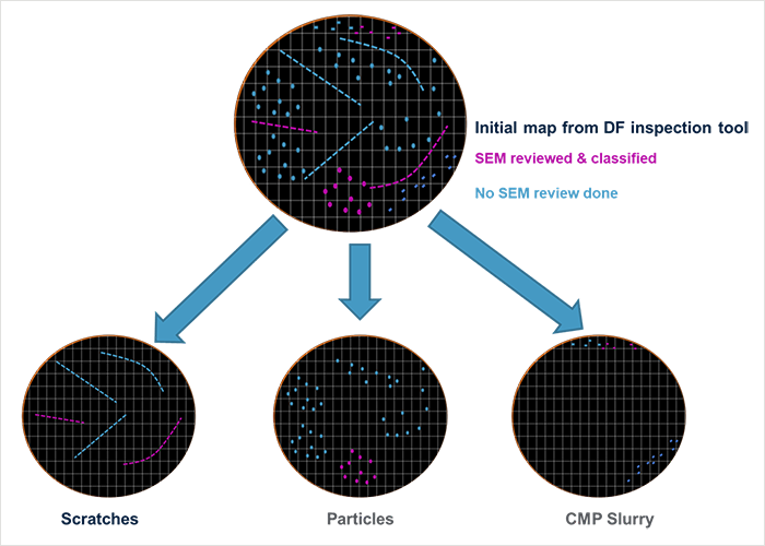
Binning helps to separate different defect types based on optical images
When many functioning chips are inaccurately marked as bad, chipmakers refer to this as “overkill.” Likewise, “underkill” is when many non-functioning chips are marked as good. It’s critical for automotive chipmakers to control and minimize both overkill and underkill.
Optical wafer inspection technologies can help by quickly producing “on-the-fly” images of each defect. This approach allows chipmakers to use attributes within the optical image to bin defects more accurately in the inspection phase, thereby minimizing the number of wafers that need to be sent to eBeam review – a complementary technology that has much higher resolution but requires more time to scan each wafer. Correctly binning defects during inspection can allow chipmakers to save hours of time that would have been spent on eBeam review – accelerating time-to-resolution and saving production costs.
Another challenge for automotive fabs is inspecting smaller chips. While leading-edge logic chips such as GPUs are growing in size, automotive chipmakers produce much smaller chips, on the order of 1mm x 1mm or even smaller. Smaller size means many more chips must be inspected on each wafer, which can slow down inspection times and ultimately impact overall fab throughput. This is another area that requires new solutions.
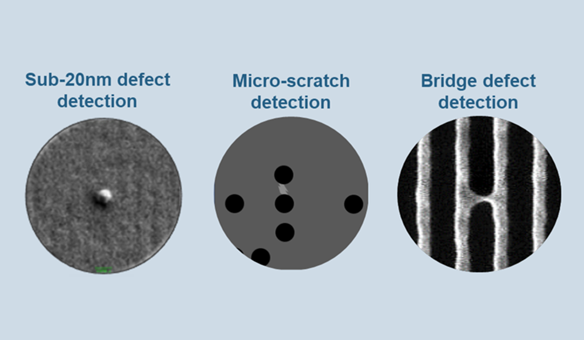
Our new darkfield inspection system is positioned to offer the best throughput-to-resolution ratio in the industry, while delivering nearly twice the data-processing rate at the same throughput as other industry offerings, permitting better defect classification and binning performance. At the same time, our unique optics enables pixel-level differentiation between defect types, which results in more accurate binning. We have several ongoing engagements with ICAPS customers to help them evaluate the technology and determine how this new capability can solve their fab process and yield challenges, enabling more reliable and better-performing chips.
1S&P Global Mobility, May 23, 2022
Ganga Sivaraman
Product Marketing Director, Optical Patterned Wafer Inspection

Gangadharan (Ganga) Sivaraman is Product Marketing Director for the Optical Patterned Wafer Inspection division at Applied Materials. Prior to joining Applied, he held various application engineering, marketing and program management roles at KLA. Ganga's experience and expertise spans FEOL/BEOL process control solutions and yield improvement methodologies. He holds a master’s degree in electrical engineering from Texas Tech University.

Semiconductor R&D Leaders Share Vision for Accelerating Advanced Packaging
One of the primary hurdles to unlocking next-generation AI is the energy-efficient performance of chips. Advanced packaging technologies such as 2.5D and 3D integration are at the forefront of this effort.
To address the challenges and opportunities of advanced packaging, Applied Materials hosted the inaugural Leadership Summit for Advanced Packaging as part of our EPIC Advanced Packaging announcement in Singapore.

Expert Panel To Explore Advances in eBeam Technology
What’s New: Alongside the 2025 SPIE Advanced Lithography + Patterning conference in San Jose, CA, Applied Materials will bring together a panel of experts from across the semiconductor ecosystem to explore how chipmakers are increasingly using electron beam (eBeam) technology to continue pushing chip scaling to its limits. The discussion – featuring experts from IBM, imec, Intel and Samsung – will highlight emerging challenges in the “angstrom era” of chipmaking.
Advanced Logic and Memory Need New Tools for Optical Wafer Inspection
The journey from R&D to high-volume manufacturing is a race, and whoever crosses the finish line first wins competitive advantage in terms of revenue, market share and profitability. Advanced chips are built up one layer at a time, and each of the billions of individual features must be perfectly patterned and aligned to create working transistors and interconnects with the best performance and power characteristics.